PN3566
PN3566
NPN General Purpose Amplifier
• This device is for use as a medium amplifier and switch requiring collect...
PN3566
PN3566
NPN General Purpose Amplifier
This device is for use as a medium amplifier and switch requiring collector currents up 300mA. Sourced from process 19.
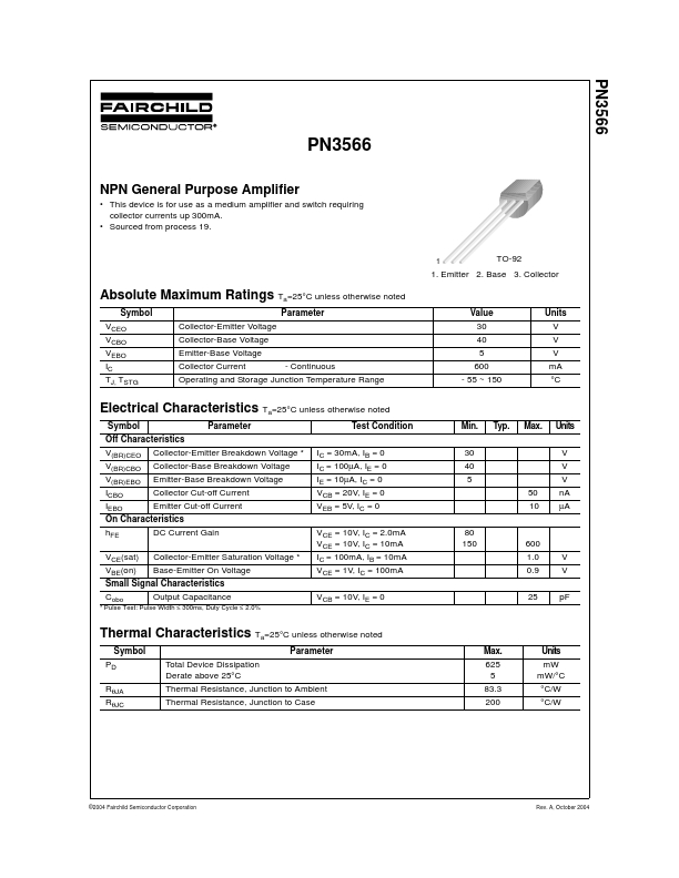
1
TO-92
1. Emitter 2. Base 3. Collector
Absolute Maximum Ratings Ta=25°C unless otherwise noted
Symbol VCEO VCBO VEBO IC TJ, TSTG Parameter Collector-Emitter
Voltage Collector-Base
Voltage Emitter-Base
Voltage Collector Current - Continuous Operating and Storage Junction Temperature Range Value 30 40 5 600 - 55 ~ 150 Units V V V mA °C
Electrical Characteristics Ta=25°C unless otherwise noted
Symbol Parameter Test Condition IC = 30mA, IB = 0 IC = 100µA, IE = 0 IE = 10µA, IC = 0 VCB = 20V, IE = 0 VEB = 5V, IC = 0 VCE = 10V, IC = 2.0mA VCE = 10V, IC = 10mA IC = 100mA, IB = 10mA VCE = 1V, IC = 100mA VCB = 10V, IE = 0 80 150 Min. 30 40 5 50 10 Typ. Max. Units V V V nA µA Off Characteristics V(BR)CEO Collector-Emitter Breakdown
Voltage * V(BR)CBO V(BR)EBO ICBO IEBO Collector-Base Breakdown
Voltage Emitter-Base Breakdown
Voltage Collector Cut-off Current Emitter Cut-off Current
On Characteristics hFE DC Current Gain VCE(sat) VBE(on) Collector-Emitter Saturation
Voltage * Base-Emitter On
Voltage
600 1.0 0.9 25 V V pF
Small Signal Characteristics Cobo Output Capacitance
* Pulse Test: Pulse Width ≤ 300ms, Duty Cycle ≤ 2.0%
Thermal Characteristics Ta=25°C unless otherwise noted
Symbol PD RθJA RθJC Parameter Total Device Dissipation Derate above 25°C Thermal Resistance, Junction to Ambient Thermal Resistance, Jun...