m o .c U 4 t e FEATURES e h • Full CMOS output swing with 40-mA output drive S output capability. 25-mA drive at TTL lev...
m o .c U 4 t e FEATURES e h Full
CMOS output swing with 40-mA output drive S output capability. 25-mA drive at TTL level. a t Advanced, low power, sub-micron
CMOS processes. a 25MHz .D fundamental crystal or clock input. 4 outputs fixed at 50MHz with output disable, 1 output w selectable at 25MHz or 100MHz with output disable w SDRAM selectable frequencies of 66.6, 75, 83.3, 100MHz w (Double Drive Strength).
PLL650-03
Low EMI Network LAN Clock
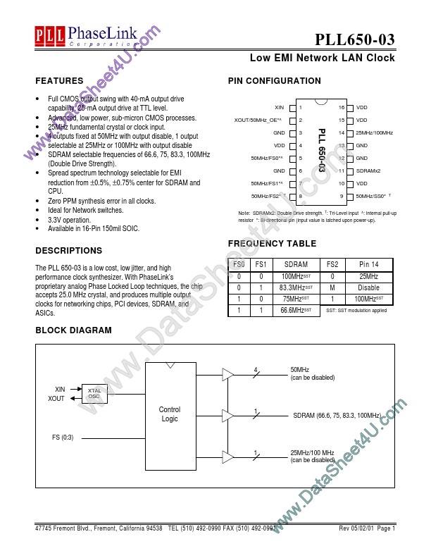
PIN CONFIGURATION
XIN XOUT/50MHz_OE*^ GND VDD 1 2 16 15 VDD VDD 25MHz/100MHz GND GND SDRAMx2 VDD 50MHz/SS0*
T
PLL 650-03
3 4 5 6 7 8
14 13 12 11 10 9
Spread spectrum technology selectable for EMI reduction from ±0.5%, ±0.75% center for SDRAM and CPU. Zero PPM synthesis error in all clocks. Ideal for Network switches. 3.3V operation. Available in 16-Pin 150mil SOIC.
DESCRIPTIONS
The PLL 650-03 is a low cost, low jitter, and high performance clock synthesizer. With PhaseLink’s proprietary analog Phase Locked Loop techniques, the chip accepts 25.0 MHz crystal, and produces multiple output clocks for networking chips, PCI devices, SDRAM, and ASICs.
BLOCK DIAGRAM
XIN XOUT
XTAL OSC
m o .c U 4 t e e h S a t a .D w w w
50MHz/FS0*^ GND 50MHz/FS1*^ 50MHz/FS2*
T
Note: SDRAMx2: Double Drive strength. T: Tri-Level input ^: Internal pull-up resistor *: Bi-directional pin (input value is latched upon power-up).
FREQUENCY TABLE
FS0 0 1 1 0 FS1 0 0 1 1 SDRAM
FS2 0 M 1
Pin 14 25MHz Disable
100MHzSST 75MHzSST
83.3MHz S...