Motherboard Clock Generator
FEATURES
• •
w w•
• • • • • • •
w
Generates all clock frequencies for VIA K7 chip sets requiring multiple CPU clocks ...
Description
FEATURES
w w
w
Generates all clock frequencies for VIA K7 chip sets requiring multiple CPU clocks and high speed SDRAM buffers. Support one pair of differential CPU clocks, one open-drain CPU, 6 PCI and 13 high-speed SDRAM buffers for 3-DIMM applications. One 24_48MHz clock and one 48MHz clock. Two14.318MHz reference clocks. Power management control to stop CPU, and Power down Mode from I2C programming. Support 2-wire I2C serial bus interface with builtin Vendor ID, Device ID and Revision ID. Single byte micro-step linear Frequency Programming via I2C with Glitch free smooth switching. Spread Spectrum ± 0.25% center spread, 0 to − 0.5% downspread. 50% duty cycle with low jitter. Available in 300 mil 48 pin SSOP.
.D
at
h S a
t e e
4U
.
m o c
PLL205-01
Motherboard Clock Generator for AMD - K7
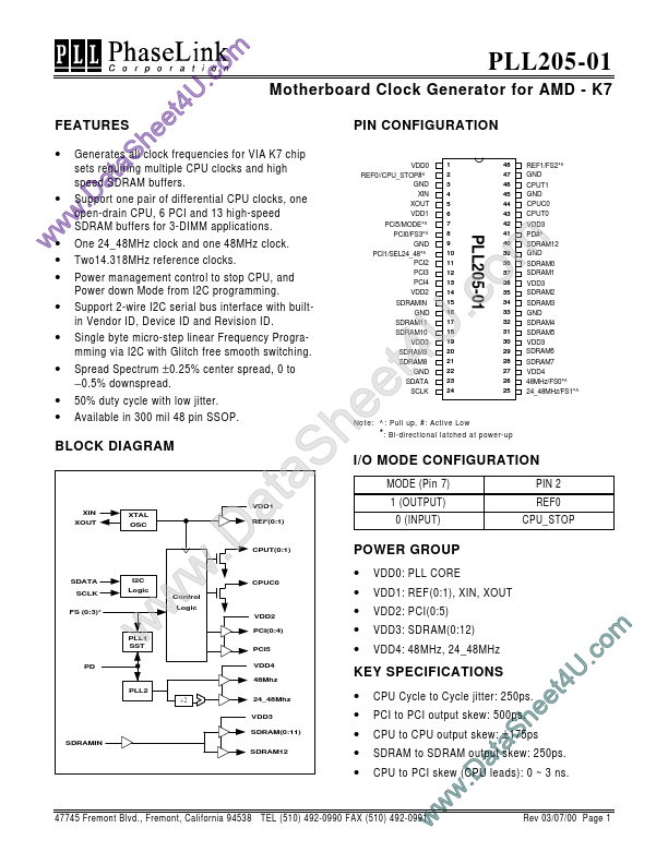
PIN CONFIGURATION
VDD0 REF0//CPU_STOP#^ GND XIN XOUT VDD1 PCI5/MODE*^ PCI0/FS3*^ GND PCI1/SEL24_48*^ PCI2 PCI3 PCI4 VDD2 SDRAMIN GND SDRAM11 SDRAM10 VDD3 SDRAM9 SDRAM8 GND SDATA SCLK
1 2 3 4 5 6 7 8 9 10 11 12 13 14 15 16 17 18 19 20 21 22 23 24 48 47 46 45 44 43 42 41 40 39 38 37 36 35 34 33 32 31 30 29 28 27 26 25
BLOCK DIAGRAM
VDD1 XIN XOUT XTAL OSC
SDATA SCLK FS (0:3)*
I2C Logic
PLL1 SST PD
w
w
÷2
Control Logic
w
.D
REF(0:1)
t a
S a
e h
t e
U 4
.c
m o
REF1/FS2*^ GND CPUT1 GND CPUC0 CPUT0 VDD3 PD#^ SDRAM12 GND SDRAM0 SDRAM1 VDD3 SDRAM2 SDRAM3 GND SDRAM4 SDRAM5 VDD3 SDRAM6 SDRAM7 VDD4 48MHz/FS0*^ 24_48MHz/FS1*^
Note: ^ : Pull up...
Similar Datasheet