Preliminary
PLL103-04
1-to-4 Clock Distribution Buffer
FEATURES
4 outputs identical to FIN. Low skew (< 250 ps between...
Preliminary
PLL103-04
1-to-4 Clock Distribution Buffer
FEATURES
4 outputs identical to FIN. Low skew (< 250 ps between outputs). Input / Output frequency range 0 – 160 MHz 25mA drive capability at TTL levels. 70mA drive capability at
CMOS levels. Output enable mode available to tri-state all outputs. www.DataSheet4U.com 3.3V operation. Available in 8-Pin 150mil SOIC.
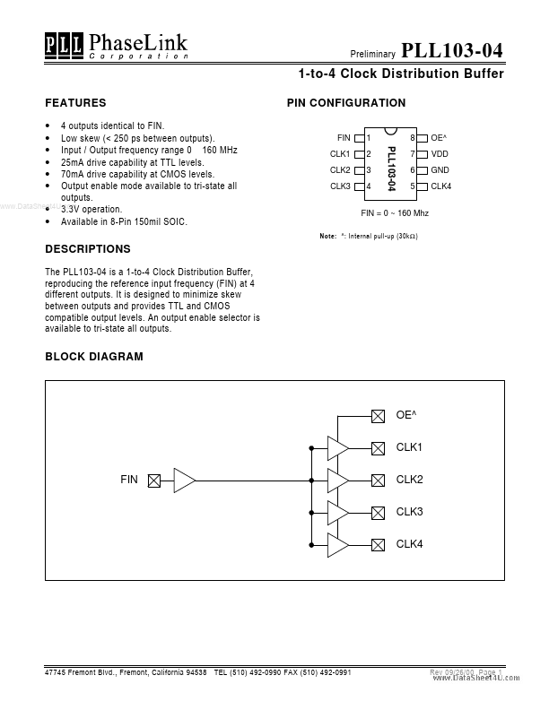
PIN CONFIGURATION
FIN CLK1 CLK2 CLK3 1 8 OE^ VDD GND CLK4
PLL103-04
2 3 4
7 6 5
FIN = 0 ~ 160 Mhz
Note: ^: Internal pull-up (30k Ω )
DESCRIPTIONS
The PLL103-04 is a 1-to-4 Clock Distribution Buffer, reproducing the reference input frequency (FIN) at 4 different outputs. It is designed to minimize skew between outputs and provides TTL and
CMOS compatible output levels. An output enable selector is available to tri-state all outputs.
BLOCK DIAGRAM
OE^ CLK1 FIN CLK2 CLK3 CLK4
47745 Fremont Blvd., Fremont, California 94538 TEL (510) 492-0990 FAX (510) 492-0991
Rev 09/26/00 Page 1
Preliminary
PLL103-04
1-to-4 Clock Distribution Buffer
PIN DESCRIPTIONS
Name
FIN CLK1 CLK2 CLK3 CLK4 www.DataSheet4U.com GND VDD OE
Number
1 2 3 4 5 6 7 8
Type
I O O O O P P I Buffered Clock Output. Buffered Clock Output. Buffered Clock Output. Buffered Clock Output. Ground. 3.3V Power Supply.
Description
Input Clock Frequency (FIN range 0 ~ 160MHz).
Output Enable. Tri-states all outputs if low. Internal pull-up resistor of 30 k Ω
47745 Fremont Blvd., Fremont, California 94538 TEL (510) 492-0990 FAX (510) ...