19MHz to 800MHz Low Phase-Noise XO
(Preliminary) PL685-88
FE AT UR E S
19MHz to 800MHz Low Phase-Noise XO
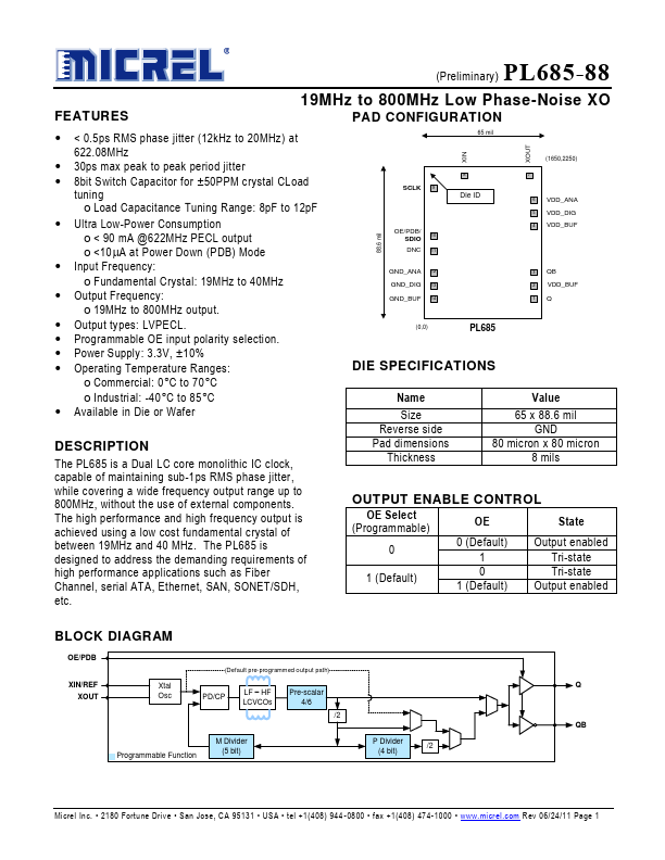
PAD CONFIGURATION
< 0.5ps RMS phase jitter (...
Description
(Preliminary) PL685-88
FE AT UR E S
19MHz to 800MHz Low Phase-Noise XO
PAD CONFIGURATION
< 0.5ps RMS phase jitter (12kHz to 20MHz) at 622.08MHz
30ps max peak to peak period jitter 8bit Switch Capacitor for ±50PPM crystal CLoad
tuning о Load Capacitance Tuning Range: 8pF to 12pF
Ultra Low-Power Consumption о < 90 mA @622MHz PECL output о <10A at Power Down (PDB) Mode
Input Frequency: о Fundamental Crystal: 19MHz to 40MHz
Output Frequency: о 19MHz to 800MHz output.
Output types: LVPECL. Programmable OE input polarity selection. Power Supply: 3.3V, ±10% Operating Temperature Ranges:
о Commercial: 0C to 70C о Industrial: -40C to 85C Available in Die or Wafer
DESCRIPTION
The PL685 is a Dual LC core monolithic IC clock, capable of maintaining sub-1ps RMS phase jitter, while covering a wide frequency output range up to 800MHz, without the use of external components. The high performance and high frequency output is achieved using a low cost fundamental crystal of between 19MHz and 40 MHz. The PL685 is designed to address the demanding requirements of high performance applications such as Fiber Channel, serial ATA, Ethernet, SAN, SONET/SDH, etc.
88.6 mil XIN XOUT
65 mil
SCLK 9
8
Die ID
OE/PDB/ SDIO
DNC
10 11
GND_ANA GND_DIG GND_BUF
12 13 14
(0,0)
PL685
(1650,2250)
7
6 VDD_ANA 5 VDD_DIG 4 VDD_BUF
3 QB 2 VDD_BUF 1Q
DIE SPECIFICATIONS
Name
Size Reverse side Pad dimensions
Thickness
Value
65 x 88.6 mil GND
80 micron x 80 micron 8 mils
OUTPUT E...
Similar Datasheet