PG 9732-B om
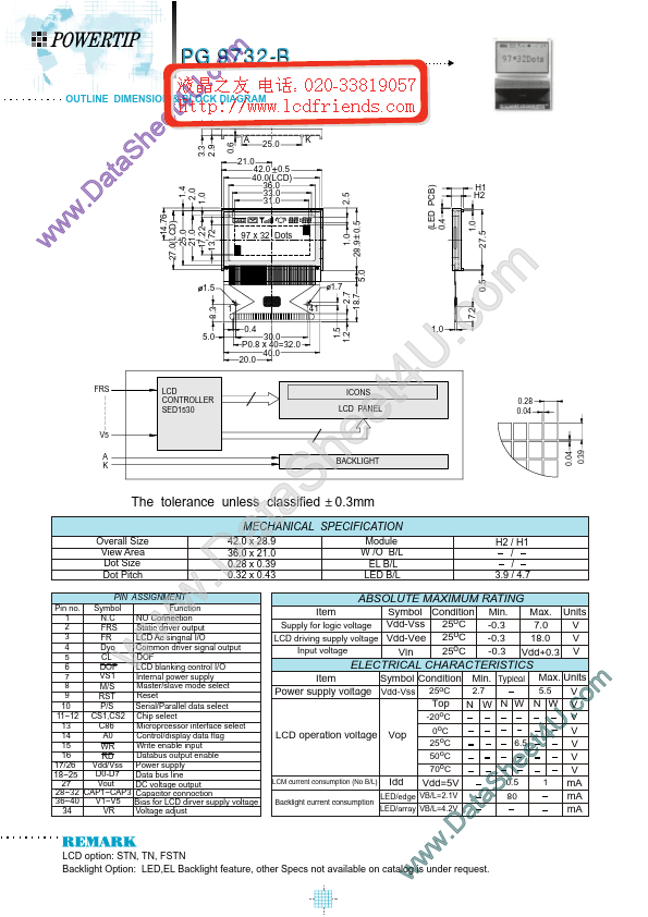
OUTLINE DIMENSION & BLOCK DIAGRAM
w
97 x 32 Dots
1.0 28.9 0.5
1.0 27.5
w
14.76 27.0(LCD) 25.0 21.0 17...
PG 9732-B om
OUTLINE DIMENSION & BLOCK DIAGRAM
w
97 x 32 Dots
1.0 28.9 0.5
1.0 27.5
w
14.76 27.0(LCD) 25.0 21.0 17.22 13.72
(LED PCB) 0.4
a D . w
S a t
3.3 2.9
e e h
U 4 t
1.4 2.0 1.0
.c
0.6
A
25.0
K
21.0 42.0 0.5 40.0(LCD) 36.0 33.0 31.0
2.5
H1 H2
2.7 18.7
1.5 8.3 1 0.4 30.0 P0.8 x 40=32.0 40.0 20.0 41
1.7 7.2
5.0
1.5 1.2
1.0
FRS
LCD CONTROLLER SED1530
ICONS
V5 A K
The tolerance unless classified
Overall Size View Area Dot Size Dot Pitch 42.0 x 28.9 36.0 x 21.0 0.28 x 0.39 0.32 x 0.43
PIN ASSIGNMENT Pin no. Symbol Function NO Connection N.C 1 2 Static driver output FRS 3 LCD Ac singnal I/O FR Dyo 4 Common driver signal output DOF 5 CL LCD blanking control I/O 6 DOF VS1 7 Internal power supply Master/slave mode select 8 M/S 9 Reset RST 10 Serial/Parallel data select P/S 11~12 CS1,CS2 Chip select 13 C86 Microprcessor interface select 14 A0 Control/display data flag Write enable input 15 WR 16 Databus output enable RD Power supply Vdd/Vss 17/26 D0-D7 18~25 Data bus line Vout 27 DC
voltage output 28~32 CAP1~CAP3 Capacitor connoction V1~V5 36~40 Bias for LCD dirver supply
voltage 34 VR
Voltage adjust
w
w
w
t a .D
MECHANICAL SPECIFICATION
Module W /O B/L EL B/L LED B/L H2 / H1 / / 3.9 / 4.7
S a
e h
0.3mm
LCD PANEL
U 4 t e
.c
m o
0.28 0.04 0.04 0.39
5.0
BACKLIGHT
ABSOLUTE MAXIMUM RATING
Item Min. -0.3 -0.3 -0.3 Max. Units V 7.0 18.0 V Vdd+0.3 V
Symbol Condition Vdd-Vss 25oC 25oC LCD driving supply
voltage Vdd-Vee Input
voltage 25oC Vin...