w
w
at .D w
h FET Power Amplifier Module for Mobile Phone MOS S a
ADE-208-461 (Z) 1st Edition July 1, 1996
ee
U 4 t...
w
w
at .D w
h FET Power Amplifier Module for Mobile Phone MOS S a
ADE-208-461 (Z) 1st Edition July 1, 1996
ee
U 4 t
m o .c
PF0031
Application
PF0031: For NMT900 890 to 925 MHz
Features
High stability: Load VSWR ≈ 20:1 Low power control current: 400 µA Thin package: 5 mm t
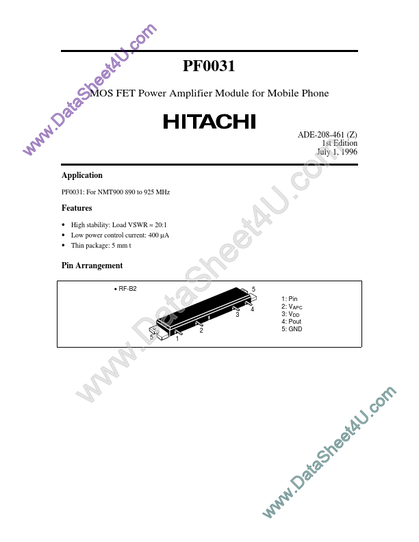
Pin Arrangement
RF-B2
w
w
.D w
5
t a
1
S a
2
e h
3
t e
5 4
U 4
.c
m o
1: Pin 2: VAPC 3: VDD 4: Pout 5: GND
w
w
w
.D
a
S a t
e e h
U 4 t
m o .c
PF0031
Internal Diagram and External Circuit
G GND Pin1 Pin Pin2 VAPC Pin3 VDD Pin4 Pout
G GND
Z1
C1
FB1
C3
FB2
C2
Z2
Pin
VAPC
VDD
Pout
C1 = C2 = 0.01 µF (Ceramic chip capacitor) C3 = 10 µF (Aluminum Electrolyte Capacitor) FB = Ferrite bead BL01RN1-A62-001 (Manufacture: MURATA) or equivalent Z1 = Z2 = 50 Ω (Microstrip line)
Absolute Maximum Ratings (Tc = 25°C)
Item Supply
voltage Supply current APC
voltage Input power Operating case temperature Storage temperature Symbol VDD I DD VAPC Pin Tc (op) Tstg Rating 17 3 8 20 –30 to +100 –40 to +110 Unit V A V mW °C °C
2
PF0031
Electrical Characteristics (Tc = 25°C)
Item Drain cutoff current Total efficiency Symbol I DS ηT Min — 35 — — — — Typ — 40 –50 –50 1.5 1.5 Max 500 — –30 –30 3 — Unit µA % dB dB — — Pin = 2 mW, VDD = 12.5 V, Pout = 6 W (at APC controlled), RL = Rg = 50 Ω, Output VSWR = 20:1 All phases, t = 20sec Test Condition VDD = 17 V, VAPC = 0 V, Rg = RL= 50 Ω Pin = 2 mW, VDD = 12.5 V, Pout = 6 W (at APC controlled) RL = Rg = 50 Ω
2nd harmonic distortion 2nd H....