STP5NA60 STP5NA60FI
N - CHANNEL ENHANCEMENT MODE FAST POWER MOS TRANSISTOR
TYPE STP5NA60 STP5NA60FI
s s s s s s s
V DSS...
STP5NA60 STP5NA60FI
N - CHANNEL ENHANCEMENT MODE FAST POWER MOS TRANSISTOR
TYPE STP5NA60 STP5NA60FI
s s s s s s s
V DSS 600 V 600 V
R DS( on) < 1.6 Ω < 1.6 Ω
ID 5.3 A 3.4 A
TYPICAL RDS(on) = 1.35 Ω ± 30V GATE TO SOURCE
VOLTAGE RATING 100% AVALANCHE TESTED REPETITIVE AVALANCHE DATA AT 100oC LOW INTRINSIC CAPACITANCES GATE GHARGE MINIMIZED REDUCED THRESHOLD
VOLTAGE SPREAD TO-220
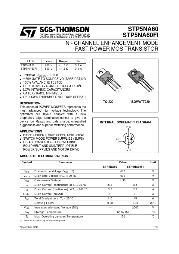
3 1 2 1 2
3
DESCRIPTION This series of POWER
MOSFETS represents the most advanced high
voltage technology. The optimized cell layout coupled with a new proprietary edge termination concur to give the device low RDS(on) and gate charge, unequalled ruggedness and superior switching performance. APPLICATIONS HIGH CURRENT, HIGH SPEED SWITCHING s SWITCH MODE POWER SUPPLIES (SMPS) s DC-AC CONVERTERS FOR WELDING EQUIPMENT AND UNINTERRUPTIBLE POWER SUPPLIES AND MOTOR DRIVE
s
ISOWATT220
INTERNAL SCHEMATIC DIAGRAM
ABSOLUTE MAXIMUM RATINGS
Symbol Parameter STP5NA60 VD S V DG R V GS ID ID ID M( ) P tot V ISO T stg Tj Drain-source
Voltage (V GS = 0) Drain-gate
Voltage (RG S = 20 k Ω ) Gate-source
Voltage Drain Current (continuous) at T c = 25 C Drain Current (continuous) at T c = 100 oC Drain Current (pulsed) Total Dissipation at Tc = 25 C Derating Factor Insulation Withstand
Voltage (DC) Storage Temperature Max. Operating Junction Temperature
o o
Value STP5NA60FI 600 600 ± 30 5.3 3.5 21 110 0.88 -65 to 150 150 3.4 2.3 21 45 0.36 2000
Unit
V V V A A A W W/o C V
o o
C C
() Pulse width limited by sa...