www.DataSheet4U.com
NIKO-SEM
N- & P-Channel Enhancement Mode Field Effect Transistor(Preliminary)
P4532VG
SOP-8 Lead-...
www.DataSheet4U.com
NIKO-SEM
N- & P-Channel Enhancement Mode Field Effect Transistor(Preliminary)
P4532VG
SOP-8 Lead-Free
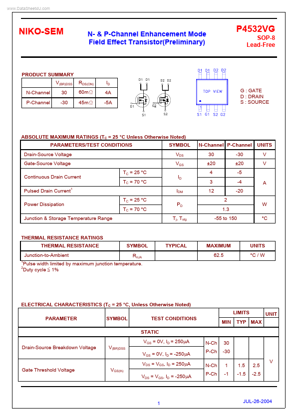
PRODUCT SUMMARY V(BR)DSS N-Channel P-Channel 30 -30 RDS(ON) 60mΩ 45mΩ ID 4A -5A G : GATE D : DRAIN S : SOURCE
ABSOLUTE MAXIMUM RATINGS (TC = 25 °C Unless Otherwise Noted) PARAMETERS/TEST CONDITIONS Drain-Source
Voltage Gate-Source
Voltage Continuous Drain Current Pulsed Drain Current Power Dissipation Junction & Storage Temperature Range
1
SYMBOL VDS VGS
N-Channel P-Channel 30 ±20 4 3 12 2 1.3 -55 to 150 -30 ±20 -5 -4 -20
UNITS V V
TC = 25 °C TC = 70 °C TC = 25 °C TC = 70 °C
ID IDM PD Tj, Tstg
A
W °C
THERMAL RESISTANCE RATINGS THERMAL RESISTANCE Junction-to-Ambient
1 2
SYMBOL RθJA
TYPICAL
MAXIMUM 62.5
UNITS °C / W
Pulse width limited by maximum junction temperature. Duty cycle ≤ 1%
ELECTRICAL CHARACTERISTICS (TC = 25 °C, Unless Otherwise Noted) LIMITS PARAMETER SYMBOL TEST CONDITIONS STATIC Drain-Source Breakdown
Voltage V(BR)DSS VGS = 0V, ID = 250µA VGS = 0V, ID = -250µA Gate Threshold
Voltage VGS(th) VDS = VGS, ID = 250µA VDS = VGS, ID = -250µA N-Ch P-Ch N-Ch P-Ch 30 -30 1 -1 1.5 -1.5 2.5 -2.5 V MIN TYP MAX UNIT
1
JUL-26-2004
NIKO-SEM
N- & P-Channel Enhancement Mode Field Effect Transistor(Preliminary)
P4532VG
SOP-8 Lead-Free
VDS = 0V, VGS = ±20V Gate-Body Leakage IGSS VDS = 0V, VGS = ±20V VDS = 24V, VGS = 0V VDS = -24V, VGS = 0V Zero Gate
Voltage Drain Current IDSS
N-Ch P-Ch N-Ch P-Ch
±100 ±100 1 -1 10 -10 12 -20 72 58 48 34 1...