NIKO-SEM
N-Channel High Voltage Mode
Field Effect Transistor
P1160ZTF:TO-220F P1160ZTFS:TO-220FS
Halogen-Free & Lead-F...
NIKO-SEM
N-Channel High
Voltage Mode
Field Effect Transistor
P1160ZTF:TO-220F P1160ZTFS:TO-220FS
Halogen-Free & Lead-Free
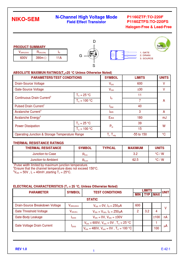
PRODUCT SUMMARY
V(BR)DSS
RDS(ON)
600V
390mΩ
ID 11A
D G
S
ABSOLUTE MAXIMUN RATINGS(TA=25 °C Unless Otherwise Noted)
PARAMETERS/TEST CONDITIONS
SYMBOL
Drain-Source
Voltage Gate-Source
Voltage
Continuous Drain Current2
Pulsed Drain Current1 Avalanche Current3 Avalanche Energy3
TC = 25 °C TC = 100 °C
VDS VGS
ID
IDM IAS EAS
Power Dissipation
TC = 25 °C TC = 100 °C
Operating Junction & Storage Temperature Range
PD Tj, Tstg
THERMAL RESISTANCE RATINGS THERMAL RESISTANCE
SYMBOL
TYPICAL
Junction-to-Case
RJc
Junction-to-Ambient
RJA
1Pulse width limited by maximum junction temperature. 2Ensure that the channel temperature does not exceed 150°C. 3VDD = 50V , L = 40mH ,starting TJ = 25°C.
1 23
1. GATE 2. DRAIN 3. SOURCE
LIMITS 600 ±30 11 7 40 3 180 39 15
-55 to 150
UNITS V V
A
A mJ W °C
MAXIMUM 3.2 62.5
UNITS °C / W °C / W
ELEC...