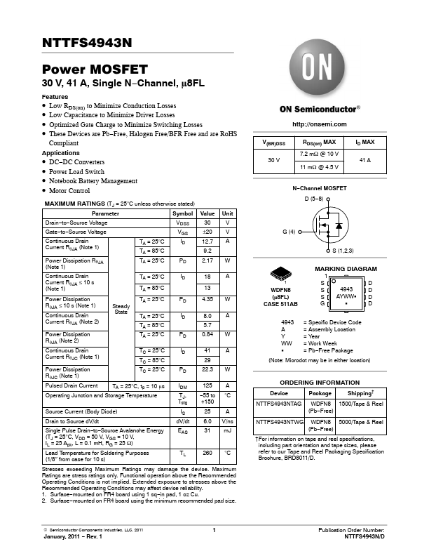
NTTFS4943N
Power MOSFET
30 V, 41 A, Single N−Channel, m8FL
Features
• Low RDS(on) to Minimize Conduction Losses • Low ...
NTTFS4943N
Power
MOSFET
30 V, 41 A, Single N−Channel, m8FL
Features
Low RDS(on) to Minimize Conduction Losses Low Capacitance to Minimize Driver Losses Optimized Gate Charge to Minimize Switching Losses These Devices are Pb−Free, Halogen Free/BFR Free and are RoHS
Compliant
Applications
DC−DC Converters Power Load Switch Notebook Battery Management Motor Control
MAXIMUM RATINGS (TJ = 25°C unless otherwise stated)
Parameter
Symbol Value Unit
Drain−to−Source
Voltage Gate−to−Source
Voltage Continuous Drain Current RqJA (Note 1)
Power Dissipation RqJA (Note 1)
VDSS
30
V
VGS
±20 V
TA = 25°C
ID
12.7 A
TA = 85°C
9.2
TA = 25°C
PD
2.17 W
Continuous Drain Current RqJA ≤ 10 s (Note 1)
TA = 25°C
ID
TA = 85°C
18
A
13
Power Dissipation RqJA ≤ 10 s (Note 1)
Continuous Drain Current RqJA (Note 2)
Steady State
TA = 25°C
TA = 25°C TA = 85°C
Power Dissipation RqJA (Note 2)
TA = 25°C
Continuous Drain Current RqJC (Note 1)
TC = 25°C TC = 85°C
Power Dissipation RqJC (Note 1)
TC = 25°C
Pulsed Drain Current
TA = 25°C, tp = 10 ms
Operating Junction and Storage Temperature
Source Current (Body Diode) Drain to Source dV/dt
PD
4.35 W
ID
8.0
A
5.7
PD
0.84 W
ID
41
A
29
PD
22.3 W
IDM TJ, Tstg IS dV/dt
125 A
−55 to °C +150
25
A
6.0 V/ns
Single Pulse Drain−to−Source Avalanche Energy
EAS
(TJ = 25°C, VDD = 50 V, VGS = 10 V,
IL = 25 Apk, L = 0.1 mH, RG = 25 W)
31 mJ
Lead Temperature for Soldering Purposes (1/8″ from case for 10 s)
...