NTMS4107N Power MOSFET
30 V, 18 A, Single N−Channel, SO−8
Features
www.DataSheet4U.com
• Ultra Low RDS(on) (at 4.5 VGS...
NTMS4107N Power
MOSFET
30 V, 18 A, Single N−Channel, SO−8
Features
www.DataSheet4U.com
Ultra Low RDS(on) (at 4.5 VGS), Low Gate Resistance and Low QG Optimized for Low Side Synchronous Applications High Speed Switching Capability
Applications
http://onsemi.com
V(BR)DSS 30 V RDS(on) TYP 3.4 mW @ 10 V 4.7 mW @ 4.5 V ID MAX 18 A
Notebook Computer Vcore Applications Network Applications DC−DC Converters
MAXIMUM RATINGS (TJ = 25°C unless otherwise noted)
Rating Drain−to−Source
Voltage Gate−to−Source
Voltage Continuous Drain C Current t (N (Note t 1) Steady State t v10 s Dissipation Power Dissi ation (Note 1) Steady State t v10 s Continuous Drain C rrent (Note 2) Current Dissipation Power Dissi ation (Note 2) Pulsed Drain Current Steady y State TA = 25°C TA = 85°C TA = 25°C PD TA = 25°C 2.5 TA = 25°C TA = 85°C TA = 25°C PD IDM TJ, Tstg IS EAS ID 11 8.0 0.93 56 −55 to 150 3.0 880 W A °C A mJ A Symbol VDSS VGS ID Value 30 $20 15 11 18 1.67 W Unit V V A
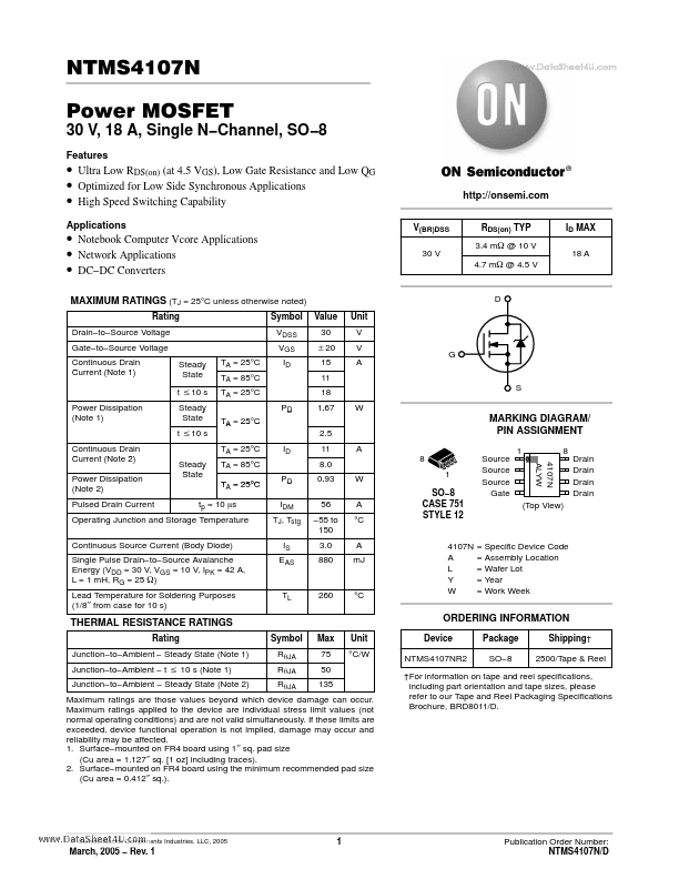
D
G
S
MARKING DIAGRAM/ PIN ASSIGNMENT
1 8 1 SO−8 CASE 751 STYLE 12 Source Source Source Gate 4107N ALYW 8 Drain Drain Drain Drain
tp = 10 ms
(Top View)
Operating Junction and Storage Temperature Continuous Source Current (Body Diode) Single Pulse Drain−to−Source Avalanche Energy (VDD = 30 V, VGS = 10 V, IPK = 42 A, L = 1 mH, RG = 25 W) Lead Temperature for Soldering Purposes (1/8″ from case for 10 s)
TL
260
°C
4107N A L Y W
= Specific Device Code = Assembly Location = Wafer Lot = Year = Work Week
THERMAL RE...