NTJS3151P, NVJS3151P
MOSFET – Power, Single, P-Channel, Trench, ESD Protected, SC-88
12 V, 3.3 A
Features
• Leading Tre...
NTJS3151P, NVJS3151P
MOSFET – Power, Single, P-Channel, Trench, ESD Protected, SC-88
12 V, 3.3 A
Features
Leading Trench Technology for Low RDS(ON) Extending Battery Life SC−88 Small Outline (2x2 mm, SC70−6 Equivalent) Gate Diodes for ESD Protection NV Prefix for Automotive and Other Applications Requiring Unique
Site and Control Change Requirements; AEC−Q101 Qualified and PPAP Capable
These Devices are Pb−Free, Halogen Free/BFR Free and are RoHS
Compliant
Applications
High Side Load Switch Cell Phones, Computing, Digital Cameras, MP3s and PDAs
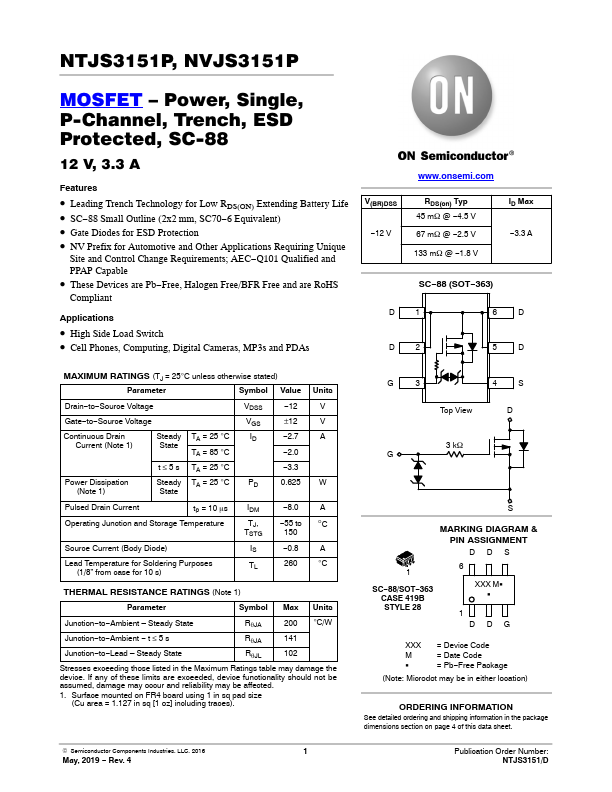
V(BR)DSS −12 V
D D
www.onsemi.com
RDS(on) Typ 45 mW @ −4.5 V 67 mW @ −2.5 V
133 mW @ −1.8 V
ID Max −3.3 A
SC−88 (SOT−363)
1 6D
2 5D
MAXIMUM RATINGS (TJ = 25°C unless otherwise stated)
Parameter
Symbol Value
Drain−to−Source
Voltage
Gate−to−Source
Voltage
Continuous Drain Current (Note 1)
Steady State
Power Dissipation (Note 1)
t≤5s Steady State
TA = 25 °C TA = 85 °C TA = 25 °C TA = 25 °C
VDSS VGS ID
PD
−12 ±12 −2.7 −2.0 −3.3 0.625
Pulsed Drain Current
tp = 10 ms
Operating Junction and Storage Temperature
Source Current (Body Diode) Lead Temperature for Soldering Purposes
(1/8” from case for 10 s)
IDM TJ, TSTG IS TL
−8.0 −55 to
150 −0.8 260
Units V V A
W
A
°C
A °C
THERMAL RESISTANCE RATINGS (Note 1)
Parameter
Symbol Max Units
Junction−to−Ambient – Steady State
RqJA
200 °C/W
Junction−to−Ambient − t ≤ 5 s
RqJA
141
Junction−to−Lead – Steady State
RqJL
102
Stresses exceeding those listed ...