NTHS4111P Power MOSFET
−30 V, −6.1 A, Single P−Channel, ChipFETt
Features
• • • • • • • • •
Offers an Ultra Low RDS(on...
NTHS4111P Power
MOSFET
−30 V, −6.1 A, Single P−Channel, ChipFETt
Features
Offers an Ultra Low RDS(on) Solution in the ChipFET Package ChipFET Package 40% Smaller Footprint than TSOP−6 Low Profile (<1.1 mm) for Extremely Thin Environments Standard Logic Level Gate Drive Pb−Free Package is Available
http://onsemi.com
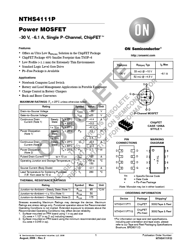
V(BR)DSS −30 V RDS(on) Typ 33 mW @ −10 V 52 mW @ −4.5 V S ID Max −6.1 A
Applications
Notebook Computer Load Switch Battery and Load Management Applications in Portable Equipment Charge Control in Battery Chargers Buck and Boost Converters
Rating Symbol VDSS VGS Steady State t ≤ 10 s Steady State t ≤ 10 s Steady State TA = 25°C TA = 85°C TA = 25°C TA = 25°C PD ID Value −30 ±20 −4.4 −3.2 −6.1 1.3 2.5 TA = 25°C TA = 85°C TA = 25°C tp = 10 ms PD IDM TJ, TSTG IS TL ID −3.3 −2.3 0.7 −30 −55 to 150 −2.1 260 W A °C A °C TH M G A W 1 Unit V V A
G
MAXIMUM RATINGS (TJ = 25°C unless otherwise noted)
Drain−to−Source
Voltage Gate−to−Source
Voltage Continuous Drain Current (Note 1) Power Dissipation (Note 1) Continuous Drain Current (Note 2) Power Dissipation (Note 2) Pulsed Drain Current D P−Channel
MOSFET 8
www.DataSheet4U.com
ChipFET CASE 1206A STYLE 1 MARKING DIAGRAM
1 2 3 4 TH M G G 8 7 6 5
PIN CONNECTIONS
D D D S
8 7 6 5 1 2 3 4
D D D G
Operating Junction and Storage Temperature Source Current (Body Diode) Lead Temperature for Soldering Purposes (1/8″ from case for 10 s)
THERMAL RESISTANCE RATINGS
Rating Junction−to−Ambient – Steady State (Not...