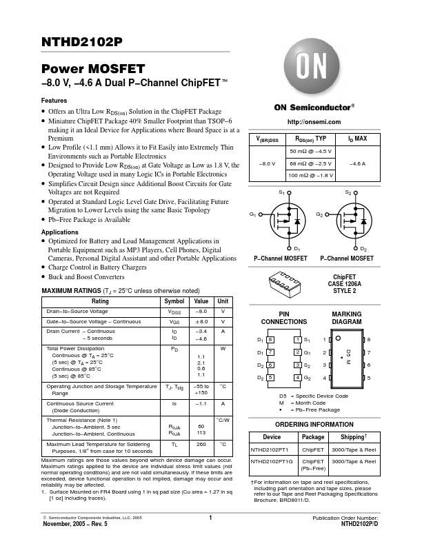
NTHD2102P
Power MOSFET
−8.0 V, −4.6 A Dual P−Channel ChipFETt
Features
• Offers an Ultra Low RDS(on) Solution in the C...
NTHD2102P
Power
MOSFET
−8.0 V, −4.6 A Dual P−Channel ChipFETt
Features
Offers an Ultra Low RDS(on) Solution in the ChipFET Package Miniature ChipFET Package 40% Smaller Footprint than TSOP−6
making it an Ideal Device for Applications where Board Space is at a Premium
Low Profile (<1.1 mm) Allows it to Fit Easily into Extremely Thin
Environments such as Portable Electronics
Designed to Provide Low RDS(on) at Gate
Voltage as Low as 1.8 V, the
Operating
Voltage used in many Logic ICs in Portable Electronics
Simplifies Circuit Design since Additional Boost Circuits for Gate
Voltages are not Required
Operated at Standard Logic Level Gate Drive, Facilitating Future
Migration to Lower Levels using the same Basic Topology
Pb−Free Package is Available
Applications
Optimized for Battery and Load Management Applications in
Portable Equipment such as MP3 Players, Cell Phones, Digital Cameras, Personal Digital Assistant and other Portable Applications
Charge Control in Battery Chargers Buck and Boost Converters
MAXIMUM RATINGS (TJ = 25°C unless otherwise noted)
Rating
Symbol Value Unit
Drain−to−Source
Voltage
Gate−to−Source
Voltage − Continuous
Drain Current − Continuous − 5 seconds
VDSS
VGS
ID ID
−8.0 "8.0 −3.4 −4.6
V V A
Total Power Dissipation
Continuous @ TA = 25°C (5 sec) @ TA = 25°C Continuous @ 85°C
(5 sec) @ 85°C
PD W
1.1 2.1 0.6 1.1
Operating Junction and Storage Temperature TJ, Tstg Range
−55 to +150
°C
Continuous Source Current (Diode Conduct...