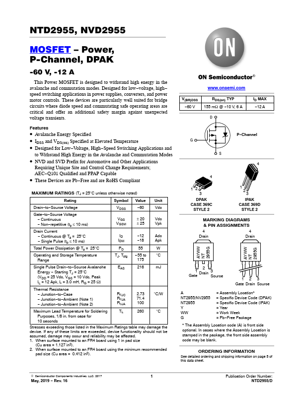
NTD2955, NVD2955
MOSFET – Power, P-Channel, DPAK
-60 V, -12 A
This Power MOSFET is designed to withstand high energy in...
NTD2955, NVD2955
MOSFET – Power, P-Channel, DPAK
-60 V, -12 A
This Power
MOSFET is designed to withstand high energy in the avalanche and commutation modes. Designed for low−
voltage, high− speed switching applications in power supplies, converters, and power motor controls. These devices are particularly well suited for bridge circuits where diode speed and commutating safe operating areas are critical and offer an additional safety margin against unexpected
voltage transients.
Features
Avalanche Energy Specified IDSS and VDS(on) Specified at Elevated Temperature Designed for Low−
Voltage, High−Speed Switching Applications and
to Withstand High Energy in the Avalanche and Commutation Modes
NVD and SVD Prefix for Automotive and Other Applications
Requiring Unique Site and Control Change Requirements; AEC−Q101 Qualified and PPAP Capable
These Devices are Pb−Free and are RoHS Compliant
MAXIMUM RATINGS (TJ = 25°C unless otherwise noted)
Rating
Symbol Value Unit
Drain−to−Source
Voltage
Gate−to−Source
Voltage − Continuous − Non−repetitive (tp ≤ 10 ms)
Drain Current Dr− Continuous @ Ta = 25°C Dr− Single Pulse (tp ≤ 10 ms)
Total Power Dissipation @ Ta = 25°C
Operating and Storage Temperature Range
VDSS VGS VGSM
−60 ± 20 ± 25
ID IDM
PD TJ, Tstg
−12 −18
55 −55 to
175
Vdc
Vdc Vpk
Adc Apk W °C
Single Pulse Drain−to−Source Avalanche Energy − Starting TJ = 25°C (VDD = 25 Vdc, VGS = 10 Vdc, Peak IL = 12 Apk, L = 3.0 mH, RG = 25 W)
Thermal Resistance − Junction−to−Case − ...