NST30010MXV6T1G, NSVT30010MXV6T1G
Dual Matched General Purpose Transistor
PNP Matched Pair
These transistors are housed...
NST30010MXV6T1G, NSVT30010MXV6T1G
Dual Matched General Purpose Transistor
PNP Matched Pair
These transistors are housed in an ultra−small SOT563 package ideally suited for portable products. They are assembled to create a pair of devices highly matched in all parameters, eliminating the need for costly trimming. Applications are Current Mirrors; Differential, Sense and Balanced
Amplifiers; Mixers; Detectors and Limiters.
Features
Current Gain Matching to 10% Base−Emitter
Voltage Matched to 2 mV Drop−In Replacement for Standard Device AEC−Q101 Qualified and PPAP Capable NSV Prefix for Automotive and Other Applications Requiring
Unique Site and Control Change Requirements
These are Pb−Free Devices*
MAXIMUM RATINGS
Rating
Symbol
Value
Unit
Collector −Emitter
Voltage
VCEO
−30
V
Collector −Base
Voltage
VCBO
−30
V
Emitter −Base
Voltage
VEBO
−5.0
V
Collector Current − Continuous
IC
−100
mAdc
Stresses exceeding Maximum Ratings may damage the device. Maximum Ratings are stress ratings only. Functional operation above the Recommended Operating Conditions is not implied. Extended exposure to stresses above the Recommended Operating Conditions may affect device reliability.
http://onsemi.com
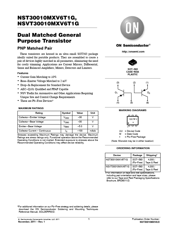
SOT−563 CASE 463A
PLASTIC
(3)
(2)
(1)
Q1
Q2
(4)
(5)
(6)
MARKING DIAGRAMS
UU M G G
1
UU = Device Code M = Date Code G = Pb−Free Package
(Note: Microdot may be in either location)
ORDERING INFORMATION
Device
Package Shipping†
NST30010MXV6T1G SOT−563 4,...