NJG1701V PHS MULTI-FUNCTION GaAs MMIC
n GENERAL DESCRIPTION NJG1701V is a GaAs multi-function MMIC composed of a power a...
NJG1701V PHS MULTI-FUNCTION GaAs MMIC
n GENERAL DESCRIPTION NJG1701V is a GaAs multi-function MMIC composed of a power amplifier, a SPDT switch and a LNA for Japanese PHS or WLL application. The SSOP20 package is adopted and effective for downsizing of handsets. NJG1701V is operated at low
voltage with low current and low distortion PA, low loss switch and low noise and high gain LNA. n APPLICATION l PHS, Digital cordless phone n FEATURES (Operating frequency f=1.9GHz) Transmitting Mode Operation l Drain
Voltage (PA) l Gain l Current consumption l Gain variable range Receiving Mode Operation l Drain
Voltage (LNA) l Gain l Current consumption l NF l Control
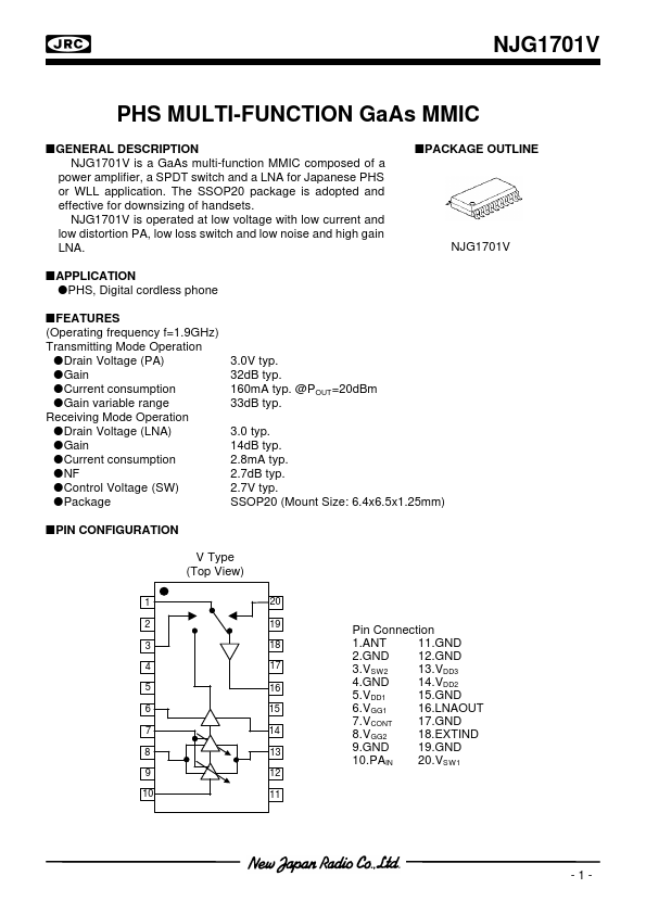
Voltage (SW) l Package n PIN CONFIGURATION V Type (Top View)
1 2 3 4 5 6 7 8 9 10 20 19 18 17 16 15 14 13 12 11
n PACKAGE OUTLINE
NJG1701V
3.0V typ. 32dB typ. 160mA typ. @POUT=20dBm 33dB typ. 3.0 typ. 14dB typ. 2.8mA typ. 2.7dB typ. 2.7V typ. SSOP20 (Mount Size: 6.4x6.5x1.25mm)
Pin Connection 1.ANT 11.GND 2.GND 12.GND 3.VSW2 13.VDD3 4.GND 14.VDD2 5.VDD1 15.GND 6.VGG1 16.LNAOUT 7.VCONT 17.GND 8.VGG2 18.EXTIND 9.GND 19.GND 10.PAIN 20.VSW1
-1-
NJG1701V
n ABSOLUTE MAXIMUM RATINGS (Zs=Zl=50Ω, Ta=25°C) PARAMETER Drain
Voltage1 Drain
Voltage2 Gate
Voltage Gain Control
Voltage Control
Voltage Input Power1 Input Power2 Power Dissipation Operating Temp. Storage Temp. SYMBOL VDD1 VDD2,3 VGG1,2 Vcont VSW1,2 ANT PAin PD Topr Tstg VDD1=3.0V, VSW1=0V, VSW2=2.7V VDD2,3=3.0V, VGG1,2=-0.9V At on PCB board VGG1,2=-0.9V VDD2,3=3.0V VDD2,...