NJG1304E
MEDIUM POWER AMPLIFIER GaAs MMIC
nGENERAL DESCRIPTION NJG1304E is a GaAs MMIC designed mainly for driver ampli...
NJG1304E
MEDIUM POWER AMPLIFIER GaAs MMIC
nGENERAL DESCRIPTION NJG1304E is a GaAs MMIC designed mainly for driver amplifier of PHS base station in Japan. This is a variable gain type with 20dB dynamic range. It features very low distortion and Pacp is less than –70dBc. at 17dBm output power ,and enable low
voltage and high efficiency operation. Small Plastic mold Package are adopted. nPACKAGE OUTLINE
NJG1304E
nFEATURES l
Voltage gain under low distortion lLow
voltage operation lLow current consumption lHigh gain lLow distortion(ACP) lPower Dissipation lReduction of Parasitic oscillation lInput and output internal matching circuit lPackage
VDD= +3.0V typ. IDD= 180mA typ. @f= 1.9GHz, Pout= 17dBm Gain= 32dB PACP= -70dBc typ. @f= 1.9GHz, POUT= 17dBm 1000mW
EMP14
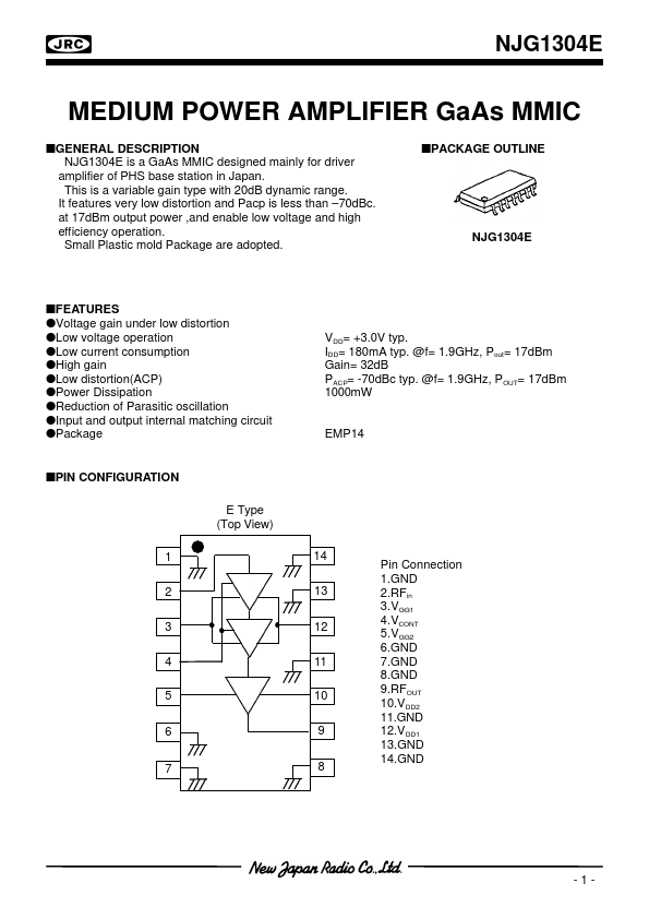
nPIN CONFIGURATION E Type (Top View) 1 2 3 4 5 6 7 14 13 12 11 10 9 8 Pin Connection 1.GND 2.RFin 3.VGG1 4.VCONT 5.VGG2 6.GND 7.GND 8.GND 9.RFOUT 10.VDD2 11.GND 12.VDD1 13.GND 14.GND
-1-
NJG1304E
nABSOLUTE MAXIMUM RATINGS PARAMETER Drain
Voltage Gate
Voltage Gain Control
Voltage Input Power Power Dissipation Operating Temperature Storage Temperature SYMBOL VDD1,VDD2 VGG1,VGG2 VCONT Pin PD Topr Tstg CONDITIONS VGG1,VGG2 =-0.9V VDD1,VDD2=-3.0V VDD1,VDD2=-3.0V VDD1,VDD2=-3.0V, VGG1,VGG2 =-0.9V At on PCB board (Ta=+25oC, Zs=Zl=50Ω) RATINGS UNITS 6.0 V -4.0 V -4.0 V 3.0 dBm 1000 mW -30 ~ +85 °C -40 ~ +150 °C
nELECTRICAL CHARACTERISTICS PARAMETER SYMBOL CONDITONS Operating Frequency freq VDD1,2=3.0V Drain
Voltage VDD1,2...