NJG1301V
MEDIUM POWER AMPLIFIER GaAs MMIC
nGENERAL DESCRIPTION NJG1301V is a medium power amplifier which is designed f...
NJG1301V
MEDIUM POWER AMPLIFIER GaAs MMIC
nGENERAL DESCRIPTION NJG1301V is a medium power amplifier which is designed for use of output stage of Japanese PHS and digital wireless phone. NJG1301V features low operating
voltage, high efficiency, and comes with, internal input and output matching circuit and very small SSOP package. This amplifier is operated up to 21dBm output level with very low noise generation. nPACKAGE OUTLINE
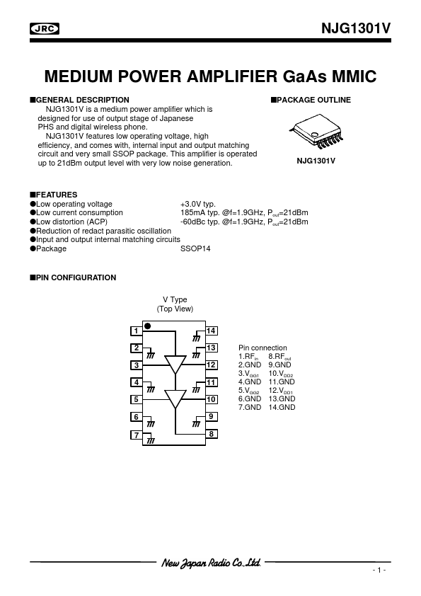
NJG1301V
nFEATURES lLow operating
voltage +3.0V typ. lLow current consumption 185mA typ. @f=1.9GHz, Pout=21dBm lLow distortion (ACP) -60dBc typ. @f=1.9GHz, Pout=21dBm lReduction of redact parasitic oscillation lInput and output internal matching circuits lPackage SSOP14
nPIN CONFIGURATION V Type (Top View) 1 2 3 4 5 6 7 14 13 12 11 10 9 8
Pin connection 1.RFin 8.RFout 2.GND 9.GND 3.VGG1 10.VDD2 4.GND 11.GND 5.VGG2 12.VDD1 6.GND 13.GND 7.GND 14.GND
-1-
NJG1301V
nABSOLUTE MAXIMUM RATINGS PARAMETER Drain
Voltage Gate
Voltage Input Power Power Dissipation Operating Temperature Storage Temperature SYMBOL VDD1,VDD2 VGG1,VGG2 Pin PD Topr Tstg CONDITIONS VGG1,VGG2 =-0.9V VDD1,VDD2=-3.0V VDD1,VDD2=-3.0V, VGG1,VGG2 =-0.9V At on PCB boad (Ta=+25°C, Zs=Zl=50Ω) RATINGS UNITS 6 V -4 V 10 dBm 600 mW -30~+85 °C -40~+150 °C
nELECTRICAL CHARACTERISTICS PARAMETER Operating Freq. Drain
Voltage Gate
Voltage Idle Current *1 Operating Current *1 Gate Current *2 Small Signal Gain Gain Flatness Pout at 1dB Gain Compression point Adjacent Channel Leakage Power 1 Adjacen...