F-42
01/99
NJ903L Process
Silicon Junction Field-Effect Transistor
¥ Low-Current ¥ Low Gate Leakage Current ¥ High In...
F-42
01/99
NJ903L Process
Silicon Junction Field-Effect Transistor
¥ Low-Current ¥ Low Gate Leakage Current ¥ High Input Impedance
Absolute maximum ratings at 25¡C free-air temperature.
Gate Current, Ig Operating Junction Temperature, Tj Storage Temperature, Ts 10 mA +150°C – 65°C to +175°C
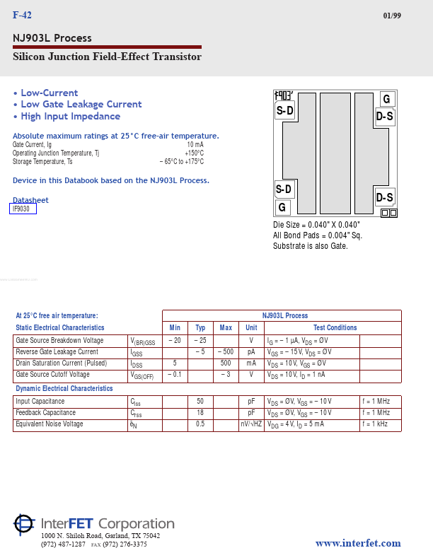
S-D
G D-S
Device in this Databook based on the NJ903L Process.
S-D
Datasheet
IF9030
G
Die Size = 0.040" X 0.040" All Bond Pads = 0.004" Sq. Substrate is also Gate.
D-S
www.DataSheet4U.com
At 25°C free air temperature: Static Electrical Characteristics Gate Source Breakdown
Voltage Reverse Gate Leakage Current Drain Saturation Current (Pulsed) Gate Source Cutoff
Voltage Dynamic Electrical Characteristics Input Capacitance Feedback Capacitance Equivalent Noise
Voltage Ciss Crss e ¯N 50 18 0.5 pF pF V(BR)GSS IGSS IDSS VGS(OFF) 5 – 0.1 Min – 20 Typ – 25 –5 – 500 500 –3 Max Unit V pA mA V
NJ903L Process Test Conditions IG = – 1 µA, VDS = ØV VGS = – 15V, VDS = ØV VDS = 10V, VGS = ØV VDS = 10V, ID = 1 nA
VDS = ØV, VGS = – 10V VDS = ØV, VGS = – 10V
f = 1 MHz f = 1 MHz f = 1 kHz
nV/√HZ VDG = 4V, ID = 5 mA
1000 N. Shiloh Road, Garland, TX 75042 (972) 487-1287 FAX (972) 276-3375
www.interfet.com
01/99
F-43
NJ903L Process
Silicon Junction Field-Effect Transistor
Drain Current as a Function of VDS
VGS(OFF) = Ð2.2 V
Gfs as a Function of VGS(OFF) 250 Transconductance in mS
250 VGS = Ø V Drain Current in mA 100 VGS = –0.5 V 150 VGS = –1.0 V 100 VGS = –1.5 V 50 VGS = –2.0 V 0 5 10 1...