www.DataSheet4U.com
NID9N05CL Power MOSFET
9.0 A, 52 V, N−Channel, Logic Level, Clamped MOSFET w/ ESD Protection in a D...
www.DataSheet4U.com
NID9N05CL Power
MOSFET
9.0 A, 52 V, N−Channel, Logic Level, Clamped
MOSFET w/ ESD Protection in a DPAK Package
http://onsemi.com Benefits
High Energy Capability for Inductive Loads Low Switching Noise Generation
Features
VDSS (Clamped) 52 V
RDS(ON) TYP 90 mΩ
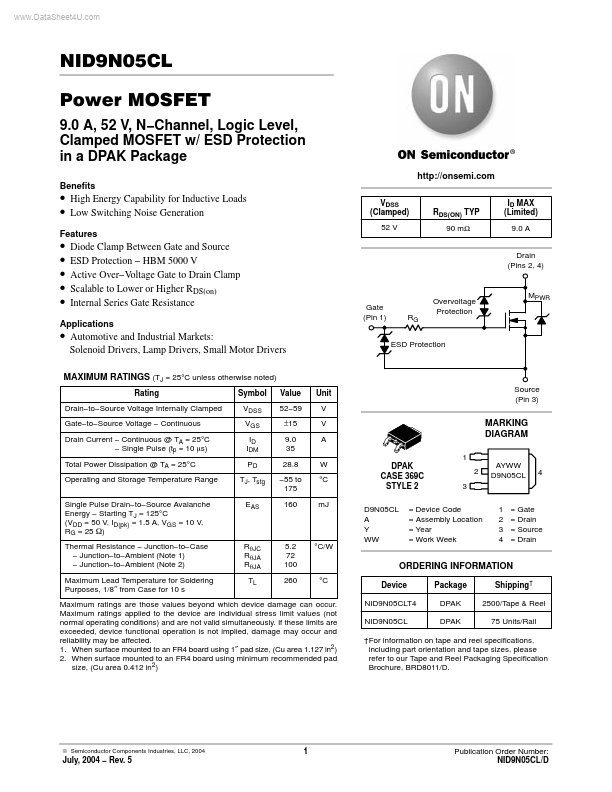
ID MAX (Limited) 9.0 A Drain (Pins 2, 4)
Diode Clamp Between Gate and Source ESD Protection − HBM 5000 V Active Over−
Voltage Gate to Drain Clamp Scalable to Lower or Higher RDS(on) Internal Series Gate Resistance
Applications
Gate (Pin 1)
RG
Over
voltage Protection
MPWR
Automotive and Industrial Markets:
Solenoid Drivers, Lamp Drivers, Small Motor Drivers
MAXIMUM RATINGS (TJ = 25°C unless otherwise noted)
Rating Drain−to−Source
Voltage Internally Clamped Gate−to−Source
Voltage − Continuous Drain Current − Continuous @ TA = 25°C Drain Current − Single Pulse (tp = 10 ms) Total Power Dissipation @ TA = 25°C Operating and Storage Temperature Range Single Pulse Drain−to−Source Avalanche Energy − Starting TJ = 125°C (VDD = 50 V, ID(pk) = 1.5 A, VGS = 10 V, RG = 25 W) Thermal Resistance − Junction−to−Case − Junction−to−Ambient (Note 1) − Junction−to−Ambient (Note 2) Maximum Lead Temperature for Soldering Purposes, 1/8″ from Case for 10 s Symbol VDSS VGS ID IDM PD TJ, Tstg EAS Value 52−59 ±15 9.0 35 28.8 −55 to 175 160 Unit V V A W °C mJ
ESD Protection
Source (Pin 3)
MARKING DIAGRAM
1 DPAK CASE 369C STYLE 2 D9N05CL A Y WW 2 3 1 2 3 4 = Gate = Drain = Source = Drain AYWW D9N05CL 4...