NPN SILICON TRANSISTOR
PRELIMINARY DATA SHEET
NPN SILICON TRANSISTOR NE856M13
FEATURES
• NEW MINIATURE M13 PACKAGE: – Small transistor outlin...
Description
PRELIMINARY DATA SHEET
NPN SILICON TRANSISTOR NE856M13
FEATURES
NEW MINIATURE M13 PACKAGE: – Small transistor outline – 1.0 X 0.5 X 0.5 mm – Low profile / 0.50 mm package height – Flat lead style for better RF performance LOW NOISE FIGURE: NF = 1.4 dB at 1 GHz HIGH COLLECTOR CURRENT: IC MAX = 100 mA
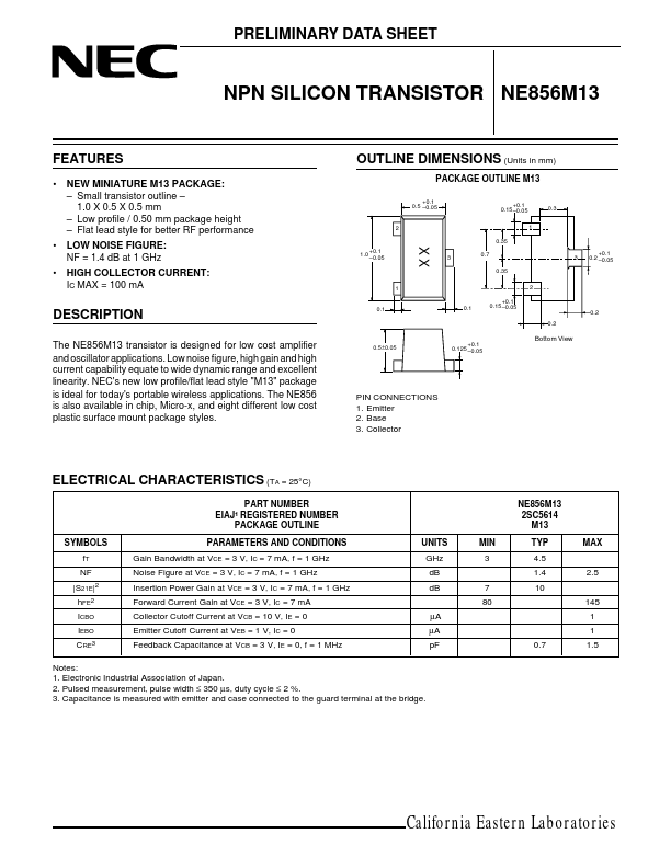
OUTLINE DIMENSIONS (Units in mm)
PACKAGE OUTLINE M13
+0.1 0.5 –0.05 +0.1 0.15 –0.05 1 0.35
0.3
2
XX
1
+0.1 1.0 –0.05
3
0.7 0.35 2 +0.1 0.15 –0.05 0.2
3
+0.1 0.2 –0.05
DESCRIPTION
The NE856M13 transistor is designed for low cost amplifier and oscillator applications. Low noise figure, high gain and high current capability equate to wide dynamic range and excellent linearity. NEC's new low profile/flat lead style "M13" package is ideal for today's portable wireless applications. The NE856 is also available in chip, Micro-x, and eight different low cost plastic surface mount package styles.
0.1
0.1
0.2
0.5±0.05
+0.1 0.125 –0.05
Bottom View
PIN CONNECTIONS 1. Emitter 2. Base 3. Collector
ELECTRICAL CHARACTERISTICS (TA = 25°C)
PART NUMBER EIAJ1 REGISTERED NUMBER PACKAGE OUTLINE SYMBOLS fT NF |S21E|2 hFE2 ICBO IEBO CRE3 PARAMETERS AND CONDITIONS Gain Bandwidth at VCE = 3 V, IC = 7 mA, f = 1 GHz Noise Figure at VCE = 3 V, IC = 7 mA, f = 1 GHz Insertion Power Gain at VCE = 3 V, IC = 7 mA, f = 1 GHz Forward Current Gain at VCE = 3 V, IC = 7 mA Collector Cutoff Current at VCB = 10 V, IE = 0 Emitter Cutoff Current at VEB = 1 V, IC = 0 Feedback Capacitance at VCB = ...
Similar Datasheet