NEC'S 10 W L & S-BAND NE650103M POWER GaAs MESFET
FEATURES
• LOW COST PLASTIC PACKAGE • USABLE TO 2.7 GHz: PCS, W-CDMA, ...
NEC'S 10 W L & S-BAND NE650103M POWER GaAs MESFET
FEATURES
LOW COST PLASTIC PACKAGE USABLE TO 2.7 GHz: PCS, W-CDMA, WLL, Satellite Uplink, BWA HIGH OUTPUT POWER: 40 dBm TYP HIGH POWER ADDED EFFICIENCY: 45 % TYP at 2.3 GHz LOW THERMAL RESISTANCE: 4.0° C/W LEAD-FREE
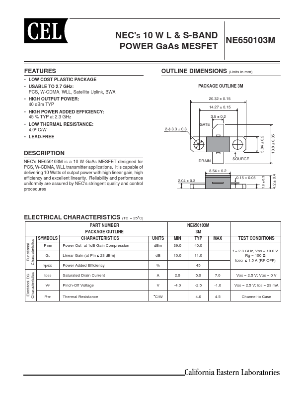
2-φ 3.3 ± 0.3 GATE
13.8 ± 0.35 4.2 ± 0.4 5.84 ± 0.2
OUTLINE DIMENSIONS (Units in mm)
PACKAGE OUTLINE 3M
20.32 ± 0.15 14.27 ± 0.15 3.5 ± 0.2
DESCRIPTION
NEC's NE650103M is a 10 W GaAs MESFET designed for PCS, W-CDMA, WLL transmitter applications. It is capable of delivering 10 Watts of output power with high linear gain, high efficiency and excellent linearity. Reliability and performance uniformity are assured by NEC's stringent quality and control procedures
DRAIN 8.54 ± 0.2 2.04 ± 0.3 0.15 ± 0.05 SOURCE
ELECTRICAL CHARACTERISTICS (TC
PART NUMBER PACKAGE OUTLINE SYMBOLS P1dB GL CHARACTERISTICS Power Out at 1dB Gain Compression Linear Gain (at Pin ≤ 23 dBm) Power Added Efficiency Saturated Drain Current Pinch-Off
Voltage Thermal Resistance
= 25°C) NE650103M 3M UNITS dBm dB % A V °C/W 2.0 -4.0 MIN 39.0 10.0 TYP 40.0 11.0 45 5.0 -2.5 4.0 7.0 -1.0 4.5 VDS = 2.5 V; VGS = 0 V VDS = 2.5 V; IDS = 23 mA Channel to Case f = 2.3 GHz, VDS = 10.0 V Rg = 100 Ω IDSQ ≤ 1.5 A (RF OFF) MAX TEST CONDITIONS
Functional Characteristics
ηADD
IDSS VP RTH
Electrical DC Characteristics
California Eastern Laboratories
1.8 ± 0.3
NE650103M ABSOLUTE MAXIMUM RATINGS1 (TC = 25 °C)
SYMBOLS VDS VGD VGS IDS IGF PT TCH TSTG PARA...