March 1996
NDS352P P-Channel Logic Level Enhancement Mode Field Effect Transistor
General Description
These P-Channel l...
March 1996
NDS352P P-Channel Logic Level Enhancement Mode Field Effect Transistor
General Description
These P-Channel logic level enhancement mode power field effect transistors are produced using Fairchild's proprietary, high cell density, DMOS technology. This very high density process is especially tailored to minimize on-state resistance. These devices are particularly suited for low
voltage applications such as notebook computer power management, portable electronics, and other battery powered circuits where fast high-side switching, and low in-line power loss are needed in a very small outline surface mount package.
Features
-0.85A, -20V. RDS(ON) = 0.5Ω @ VGS = -4.5V. Proprietary package design using copper lead frame for superior thermal and electrical capabilities. High density cell design for extremely low RDS(ON). Exceptional on-resistance and maximum DC current capability. Compact industry standard SOT-23 surface mount package.
____________________________________________________________________________________________
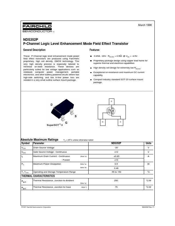
D
G
S
Absolute Maximum Ratings
Symbol VDSS VGSS ID PD TJ,TSTG Parameter Drain-Source
Voltage
T A = 25°C unless otherwise noted
NDS352P -20 ±12
(Note 1a)
Units V V A
Gate-Source
Voltage - Continuous Maximum Drain Current - Continuous - Pulsed Maximum Power Dissipation
(Note 1a) (Note 1b)
±0.85 ±10 0.5 0.46 -55 to 150
W
Operating and Storage Temperature Range
°C
THERMAL CHARACTERISTICS RθJA RθJC Thermal Resistance, Junction-to-Ambient
(...