December 1996
NDH8520C Dual N & P-Channel Enhancement Mode Field Effect Transistor
General Description
These dual N- an...
December 1996
NDH8520C Dual N & P-Channel Enhancement Mode Field Effect Transistor
General Description
These dual N- and P-Channel enhancement mode power field effect transistors are produced using Fairchild's proprietary, high cell density, DMOS technology. This very high density process is especially tailored to minimize on-state resistance and provide superior switching performance. These devices are particularly suited for low
voltage applications such as notebook computer power management and other battery powered circuits where fast switching, low in-line power loss, and resistance to transients are needed.
Features
N-Channel 2.8 A, 30 V,RDS(ON)=0.07Ω @ VGS=10 V RDS(ON)=0.1Ω @ VGS=4.5 V P-Channel -2.2 A,-30 V, RDS(ON)=0.11Ω @ VGS=-10 V RDS(ON)=0.18 Ω @ VGS=-4.5 V. Proprietary SuperSOTTM-8 package design using copper lead frame for superior thermal and electrical capabilities. High density cell design for extremely low RDS(ON). Exceptional on-resistance and maximum DC current capability.
___________________________________________________________________________________
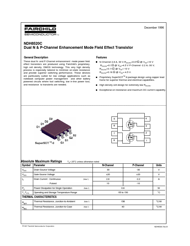
5
4 3 2
1
6
7 8
Absolute Maximum Ratings
Symbol VDSS VGSS ID Parameter Drain-Source
Voltage Gate-Source
Voltage Drain Current - Continuous - Pulsed PD TJ,TSTG
T A= 25°C unless otherwise noted
N-Channel 30 ±20
(Note 1)
P-Channel -30 ±20 -2.2 -10 0.8 -55 to 150
Units V V A
2.8 10
Power Dissipation for Single Operation Operating and Storage Temperature Range
(Note 1)
W °C
THERMAL CHARACTERIST...