April 1995
NDF0610 / NDS0610 P-Channel Enhancement Mode Field Effect Transistor
General Description
These P-Channel enh...
April 1995
NDF0610 / NDS0610 P-Channel Enhancement Mode Field Effect Transistor
General Description
These P-Channel enhancement mode power field effect transistors are produced using Fairchild's proprietary, high cell density, DMOS technology. This very high density process has been designed to minimize on-state resistance, provide rugged and reliable performance and fast switching. They can be used, with a minimum of effort, in most applications requiring up to 180mA DC and can deliver pulsed currents up to 1A. This product is particularly suited to low
voltage applications requiring a low current high side switch.
Features
-0.18 and -0.12A, -60V. RDS(ON) = 10Ω
Voltage controlled p-channel small signal switch High density cell design for low RDS(ON) TO-92 and SOT-23 packages for both through hole and surface mount applications High saturation current
____________________________________________________________________________________________
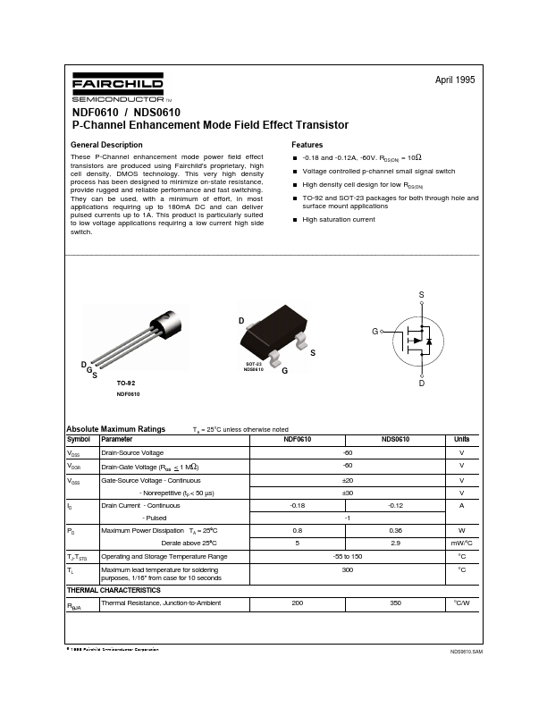
S
D
G
S
D G S
SOT-23 NDS0610
G
TO-92
NDF0610
D
Absolute Maximum Ratings
Symbol Parameter
TA = 25°C unless otherwise noted
NDF0610
NDS0610
Units
VDSS VDGR VGSS ID PD
Drain-Source
Voltage Drain-Gate
Voltage (RGS < 1 MΩ) Gate-Source
Voltage - Continuous - Nonrepetitive (tP < 50 µs) Drain Current - Continuous - Pulsed Maximum Power Dissipation TA = 25°C Derate above 25°C 0.8 5 -0.18
-60 -60 ±20 ±30 -0.12 -1 0.36 2.9 -55 to 150 300
V V V V A
W mW/oC °C °C
TJ,TSTG TL
Operating and Storage Temperature Range Maximum lead temp...