NCP5201 Dual Output DDR Power Controller
The NCP5201 Dual DDR Power Controller is specifically designed as a total power...
NCP5201 Dual Output DDR Power Controller
The NCP5201 Dual DDR Power Controller is specifically designed as a total power solution for a high current DDR memory system. This IC combines the efficiency of a PWM controller for the VDDQ supply with the simplicity of a linear regulator for the VTT memory termination
voltage. The secondary regulator (VTT) is designed to automatically track at half the primary regulator
voltage (VDDQ). An internal power good
voltage monitor tracks both VDDQ and VTT outputs and notifies the user in the event of a fault on either output. Protective features include soft−start circuitry and under
voltage monitoring of VCC and VSTBY. The IC is packaged in a 5 × 6 QFN−18.
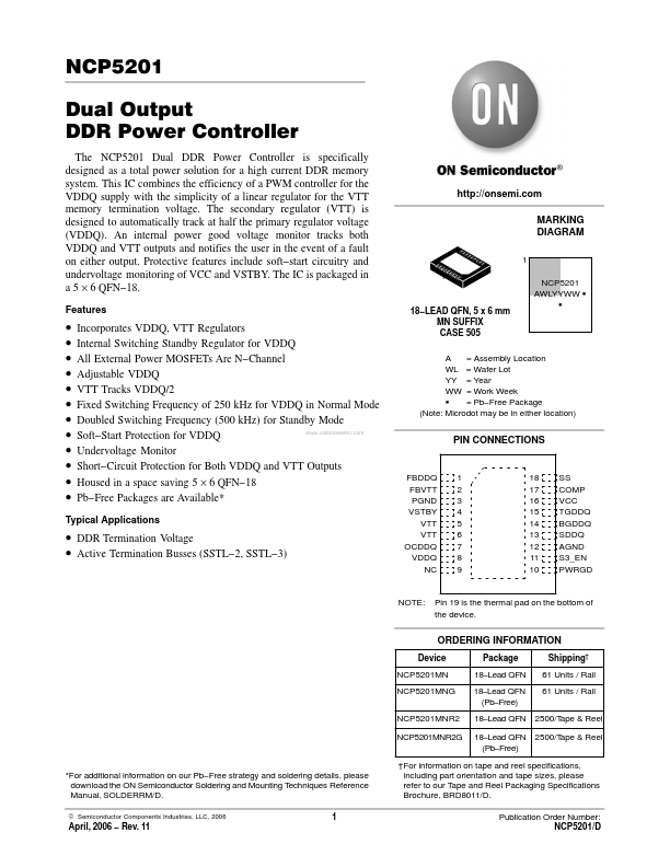
Features http://onsemi.com MARKING DIAGRAM
1 1 NCP5201 AWLYYWW G G
Incorporates VDDQ, VTT Regulators Internal Switching Standby Regulator for VDDQ All External Power
MOSFETs Are N−Channel Adjustable VDDQ VTT Tracks VDDQ/2 Fixed Switching Frequency of 250 kHz for VDDQ in Normal Mode Doubled Switching Frequency (500 kHz) for Standby Mode www.DataSheet4U.com Soft−Start Protection for VDDQ Under
voltage Monitor Short−Circuit Protection for Both VDDQ and VTT Outputs Housed in a space saving 5 × 6 QFN−18 Pb−Free Packages are Available*
18−LEAD QFN, 5 x 6 mm MN SUFFIX CASE 505
A = Assembly Location WL = Wafer Lot YY = Year WW = Work Week G = Pb−Free Package (Note: Microdot may be in either location)
PIN CONNECTIONS
Typical Applications
DDR Termination
Voltage A...