TinyLogic ULP-A 2-Input NAND Gate
NC7SV00
The NC7SV00 is a single 2−Input NAND Gate in tiny footprint packages. The devi...
TinyLogic ULP-A 2-Input NAND Gate
NC7SV00
The NC7SV00 is a single 2−Input NAND Gate in tiny footprint packages. The device is designed to operate for VCC = 0.9 V to 3.6 V.
Features
Designed for 0.9 V to 3.6 V VCC Operation 1.5 ns tPD at 3.3 V (Typ) Inputs/Outputs Over−
Voltage Tolerant up to 3.6 V IOFF Supports Partial Power Down Protection Source/Sink 24 mA at 3.3 V Available in SC−88A and MicroPak™ Packages These Devices are Pb−Free, Halogen Free/BFR Free and are RoHS
Compliant
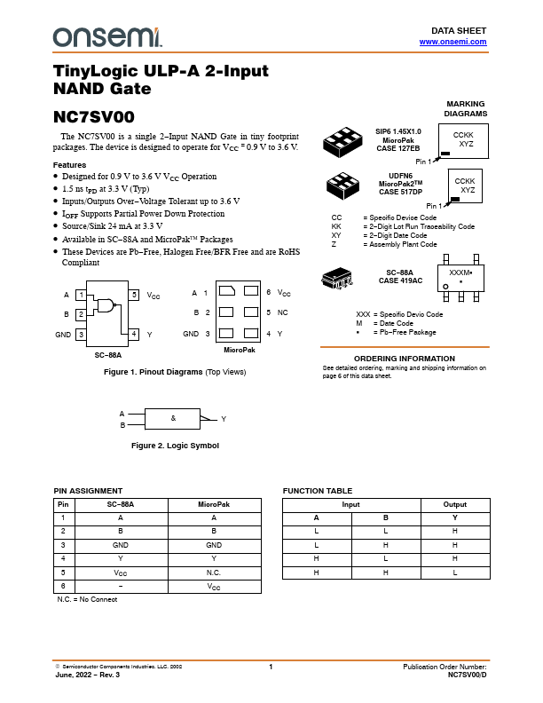
A1 B2
5 VCC
A1 B2
6 VCC 5 NC
GND 3
4Y
GND 3
4Y
SC−88A
MicroPak
Figure 1. Pinout Diagrams (Top Views)
DATA SHEET www.onsemi.com
MARKING DIAGRAMS
SIP6 1.45X1.0 MicroPak
CASE 127EB
CCKK XYZ
Pin 1
UDFN6 MicroPak2TM
CASE 517DP
CCKK XYZ
Pin 1
CC
= Specific Device Code
KK
= 2−Digit Lot Run Traceability Code
XY
= 2−Digit Date Code
Z
= Assembly Plant Code
SC−88A CASE 419AC
XXXMG G
XXX = Specific Devic Code M = Date Code G = Pb−Free Package
ORDERING INFORMATION
See detailed ordering, marking and shipping information on page 6 of this data sheet.
A
&
Y
B
Figure 2. Logic Symbol
PIN ASSIGNMENT
Pin
SC−88A
1
A
2
B
3
GND
4
Y
5
VCC
6
−
N.C. = No Connect
MicroPak A B
GND Y
N.C. VCC
FUNCTION TABLE
Input
A
B
L
L
L
H
H
L
H
H
Output Y H H H L
© Semiconductor Components Industries, LLC, 2002
1
June, 2022 − Rev. 3
Publication Order Number: NC7SV00/D
NC7SV00
MAXIMUM RATINGS
Symbol
Characteristics
Value
Unit
VCC VIN VOUT
IIK IOK IOUT ICC ...