NB6L239
2.5V / 3.3V Any Differential
Clock IN to Differential LVPECL OUT ÷1/2/4/8, ÷2/4/8/16 Clock Divider
Description ...
NB6L239
2.5V / 3.3V Any Differential
Clock IN to Differential LVPECL OUT ÷1/2/4/8, ÷2/4/8/16 Clock Divider
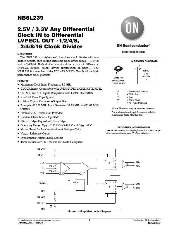
Description The NB6L239 is a high−speed, low skew clock divider with two
divider circuits, each having selectable clock divide ratios; B1/2/4/8 and B2/4/8/16. Both divider circuits drive a pair of differential LVPECL outputs. (More device information on page 7). The NB6L239 is a member of the ECLinPS MAX™ Family of the high performance clock products.
Features
Maximum Clock Input Frequency, 3.0 GHz CLOCK Inputs Compatible with LVDS/LVPECL/CML/HSTL/HCSL EN, MR, and SEL Inputs Compatible with LVTTL/LV
CMOS Rise/Fall Time 65 ps Typical < 10 ps Typical Output−to−Output Skew Example: 622.08 MHz Input Generates 38.88 MHz to 622.08 MHz
Outputs
Internal 50 W Termination Provided Random Clock Jitter < 1 ps RMS QA B1 Edge Aligned to QBBn Edge Operating Range: VCC = 2.375 V to 3.465 V with VEE = 0 V Master Reset for Synchronization of Multiple Chips VBBAC Reference Output Synchronous Output Enable/Disable These Devices are Pb−Free and are RoHS Compliant
http://onsemi.com
1
QFN−16 MN SUFFIX CASE 485G
MARKING DIAGRAM*
16
1
NB6L 239 ALYWG
G
A = Assembly Location L = Wafer Lot Y = Year W = Work Week G = Pb−Free Package
(Note: Microdot may be in either location)
*For additional marking information, refer to Application Note AND8002/D.
ORDERING INFORMATION
See detailed ordering and shipping information in the package dimensions section on page 11 of this ...