NB4N527S
3.3V, 2.5Gb/s Dual AnyLevel™ to LVDS Receiver/Driver/Buffer/ Translator with Internal Input Termination
NB4N52...
NB4N527S
3.3V, 2.5Gb/s Dual AnyLevel™ to LVDS Receiver/Driver/Buffer/ Translator with Internal Input Termination
NB4N527S is a clock or data Receiver/Driver/Buffer/Translator capable of translating AnyLevelTM input signal (LVPECL, CML, HSTL, LVDS, or LVTTL/LV
CMOS) to LVDS. Depending on the distance, noise immunity of the system design, and transmission line media, this device will receive, drive or translate data or clock signals up to 2.5 Gb/s or 1.5 GHz, respectively.
The NB4N527S has a wide input common mode range of GND + 50 mV to VCC − 50 mV combined with two 50 W internal termination resistors is ideal for translating differential or single−ended data or clock signals to 350 mV typical LVDS output levels without use of any additional external components (Figure 6).
The device is offered in a small 3 mm x 3 mm QFN−16 package. NB4N527S is targeted for data, wireless and telecom applications as well as high speed logic interface where jitter and package size are main requirements. Application notes, models, and support documentation are available on www.onsemi.com.
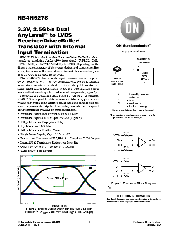
Maximum Input Clock Frequency up to 1.5 GHz Maximum Input Data Rate up to 2.5 Gb/s (Figure 5) 470 ps Maximum Propagation Delay\ 1 ps Maximum RMS Jitter 140 ps Maximum Rise/Fall Times Single Power Supply; VCC = 3.3 V $10% Temperature Compensated TIA/EIA−644 Compliant LVDS Outputs Internal 50 W Termination Resistor per Input Pin GND + 50 mV to VCC − 50 mV VCMR Range These are Pb−Free Devices
D...