Ultra-Low Skew 1:4 Clock Fanout Buffer
NB3N551
3.3 V / 5.0 V Ultra-Low Skew 1:4 Clock Fanout Buffer
Description The NB3N551 is a low skew 1−to 4 clock fanout ...
Description
NB3N551
3.3 V / 5.0 V Ultra-Low Skew 1:4 Clock Fanout Buffer
Description The NB3N551 is a low skew 1−to 4 clock fanout buffer, designed
for clock distribution in mind. The NB3N551 specifically guarantees low output−to−output skew. Optimal design, layout and processing minimize skew within a device and from device to device.
The output enable (OE) pin three−states the outputs when low.
Features
Input/Output Clock Frequency up to 180 MHz Low Skew Outputs (50 ps typical) RMS Phase Jitter (12 kHz – 20 MHz): 43 fs (Typical) Output goes to Three−State Mode via OE Operating Range: VDD = 3.0 V to 5.5 V Ideal for Networking Clocks Packaged in 8−pin SOIC Industrial Temperature Range These are Pb−Free Devices
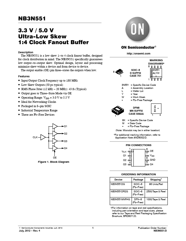
Q1
Q2 CLK
Q3
Q4
OE Figure 1. Block Diagram
http://onsemi.com
8 1
SOIC−8 D SUFFIX CASE 751
MARKING DIAGRAMS* 8
3N551 ALYW
G
1
3N551 = Specific Device Code A = Assembly Location L = Wafer Lot Y = Year W = Work Week
G = Pb−Free Packa...
Similar Datasheet