3.3 V Zero Delay Clock Buffer
NB2309A 3.3 V Zero Delay Clock Buffer
The NB2309A is a versatile, 3.3 V zero delay buffer designed to distribute high−sp...
Description
NB2309A 3.3 V Zero Delay Clock Buffer
The NB2309A is a versatile, 3.3 V zero delay buffer designed to distribute high−speed clocks. It accepts one reference input and drives out nine low−skew clocks. It is available in a 16 pin package. The −1H version of the NB2309A operates at up to 133 MHz, and has higher drive than the −1 devices. All parts have on−chip PLL’s that lock to an input clock on the REF pin. The PLL feedback is on−chip and is obtained from the CLKOUT pad. The NB2309A has two banks of four outputs each, which can be controlled by the Select inputs as shown in the Select Input Decoding Table. If all the output clocks are not required, Bank B can be three−stated. The select inputs also allow the input clock to be directly applied to the outputs for chip and system testing purposes. Multiple NB2309A devices can accept the same input clock and distribute it. In this case the skew between the outputs of the two devices is guaranteed to be less than 700 ps. All outputs have less than 200 ps of cycle−to−cycle jitter. The input and output propagation delay is guaranteed to be less than 350 ps, and the output to output skew is guaranteed to be less than 250 ps. The NB2309A is available in two different configurations, as shown in the ordering information table. The NB2309A1 is the base part. The NB2309Ax1H* is the high drive version of the −1 and its rise and fall www.DataSheet4U.com times are much faster than −1 part.
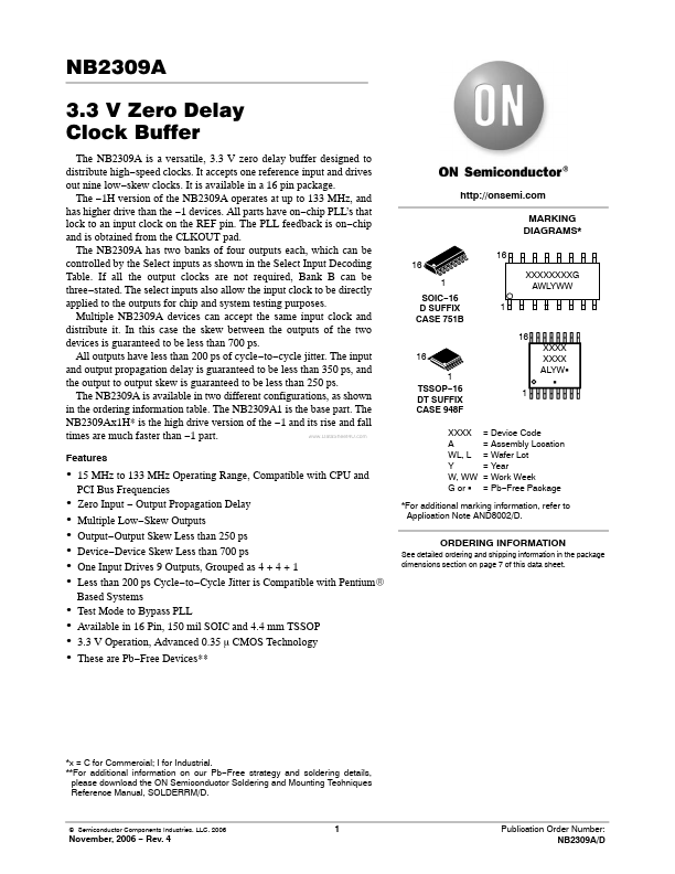
Features http://onsemi.com MARKING DIAGRAMS*
16 1 SO...
Similar Datasheet