www.DataSheet4U.com
MX23C4100
4M-BIT [512K x 8/256K x 16] MASK ROM
FEATURES
• Switchable organization - 512K x 8 (byte ...
www.DataSheet4U.com
MX23C4100
4M-BIT [512K x 8/256K x 16] MASK ROM
FEATURES
Switchable organization - 512K x 8 (byte mode) - 256K x 16 (word mode) Single +5V power supply Fast access time:100/120/150ns Totally static operation Completely TTL compatible Operating current: 60mA Standby current: 100uA Package - 40 pin DIP (600 mil) - 40 pin SOP
GENERAL DESCRIPTION
The MX23C4100 is a 5V only, 4M-bit, Read Only Memory. It is organized as 512Kx8 bits (byte mode) or as 256Kx16 bit (word mode) depending on BYTE (pin 31)
voltage level. MX23C4100 has a static standby mode, and has an access time of 100/120/150/200ns. It is designed to be compatible with all microprocessors and similar applications in which high performance, large bit storage and simple interfacing are important design considerations. MX23C4100 offers automatic power-down, with powerdown controlled by the chip enable (CE) input. When CE is not selected, the device automatically powers down and remains in a low-power standby mode as long as CE stays in the unselected mode. The OE input as well as OE input may be programmed active Low.
DataShee
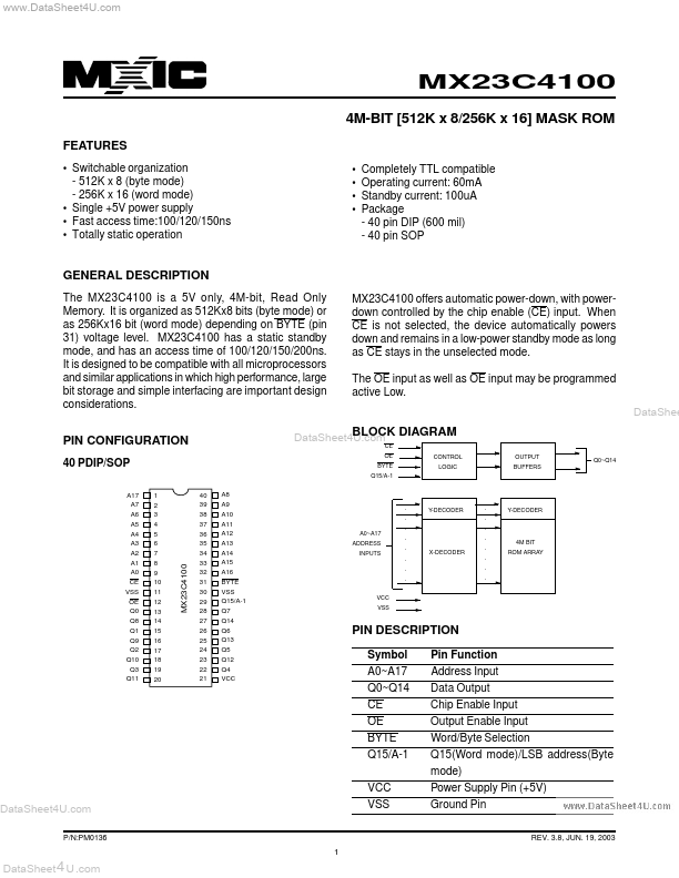
PIN CONFIGURATION
40 PDIP/SOP
A17 A7 A6 A5 A4 A3 A2 A1 A0 CE VSS OE Q0 Q8 Q1 Q9 Q2 Q10 Q3 Q11 1 2 3 4 5 6 7 8 9 10 11 12 13 14 15 16 17 18 19 20 40 39 38 37 36 35 34 33 32 31 30 29 28 27 26 25 24 23 22 21 A8 A9 A10 A11 A12 A13 A14 A15 A16 BYTE VSS Q15/A-1 Q7 Q14 Q6 Q13 Q5 Q12 Q4 VCC
DataSheet4U.com
BLOCK DIAGRAM
CE OE BYTE Q15/A-1 CONTROL LOGIC OUTPUT BUFFERS ...