MTV16N50E
Advance Information TMOS E−FET.™ Power Field Effect Transistor D3PAK for Surface Mount
N−Channel Enhancement−M...
MTV16N50E
Advance Information TMOS E−FET.™ Power Field Effect Transistor D3PAK for Surface Mount
N−Channel Enhancement−Mode Silicon Gate
This high
voltage MOSFET uses an advanced termination scheme to provide enhanced
voltage−blocking capability without degrading performance over time. In addition, this advanced TMOS E−FET is designed to withstand high energy in the avalanche and commutation modes. The new energy efficient design also offers a drain−to−source diode with a fast recovery time. Designed for high speed switching applications in power supplies, converters, PWM motor controls, these devices are particularly well suited for bridge circuits where diode speed and commutating safe operating areas are critical and offer additional safety margin against unexpected
voltage transients.
Robust High
Voltage Termination
Avalanche Energy Specified
Source−to−Drain Diode Recovery Time Comparable to a Discrete Fast Recovery Diode
Diode is Characterized for Use in Bridge Circuits IDSS and VDS(on) Specified at Elevated Temperature
http://onsemi.com
TMOS POWER FET 16 AMPERES, 500 VOLTS
RDS(on) = 0.40 W
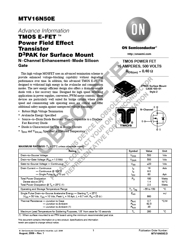
D3PAK Surface Mount CASE 433−01 Style 2
D N−Channel
®G
S
MAXIMUM RATINGS (TC = 25°C unless otherwise noted)
Rating
Drain−to−Source
Voltage
Drain−to−Gate
Voltage (RGS = 1.0 MΩ) Gate−to−Source
Voltage — Continuous
Drain Current — Continuous Drain Current — Continuous @ 100°C Drain Current — Single Pulse (tp ≤ 10 μs) Total Power Dissipation
Derate above 25°C Total Power Di...