CYStech Electronics Corp.
60V N-CHANNEL Enhancement Mode MOSFET
MTN2310N3
Spec. No. : C393N3 Issued Date : 2007.10.24 R...
CYStech Electronics Corp.
60V N-CHANNEL Enhancement Mode
MOSFET
MTN2310N3
Spec. No. : C393N3 Issued Date : 2007.10.24 Revised Date : Page No. : 1/6
Features
VDS=60V RDS(ON)=90mΩ(max.)@VGS=10V, IDS=3A
RDS(ON)=120mΩ(max.)@VGS=4.5V, IDS=2A
Simple drive requirement Small package outline
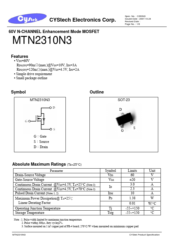
Symbol
MTN2310N3
Outline
SOT-23 D
G:Gate S:Source D:Drain
GS
Absolute Maximum Ratings (Ta=25°C)
Parameter
Drain-Source
Voltage Gate-Source
Voltage Continuous Drain Current @VGS=4.5V, TA=25°C (Note 3) Continuous Drain Current @VGS=4.5V, TA=70°C (Note 3) Pulsed Drain Current (Notes 1, 2)
Maximum Power Dissipation@ TA=25℃ Linear Derating Factor
Operating Junction Temperature Storage Temperature
Symbol VDS VGS
ID
IDM PD
Tj Tstg
Limits 60 ±20
3.0 2.3 10
1.38
0.01 -55~+150 -55~+150
Note : 1. Pulse width limited by maximum junction temperature. 2. Pulse width≤ 300μs, duty cycle≤2%.
3. Surface mounted on 1 in² copper pad of FR-4 board; 270°C/W when mounted on minimum copper pad
Unit V V
A A A
W
W/°C °C °C
MTN2310N3
CYStek Product Specification
CYStech Electronics Corp.
Spec. No. : C393N3 Issued Date : 2007.10.24 Revised Date : Page No. : 2/6
Thermal Performance
Parameter Thermal Resistance, Junction-to-Ambient(PCB mounted)
Symbol Rth,ja
Limit 90
Note : Surface mounted on 1 in² copper pad of FR-4 board; 270°C/W when mounted on minimum copper pad
Unit °C/W
Electrical Characteristics (Tj=25°C, unless otherwise noted)
Symbol
Min. Typ. Max. Unit
Test Conditions
Static BVDSS
∆BV...