CYStech Electronics Corp.
Spec. No. : C064N3 Issued Date : 2016.08.16
Revised Date : Page No. : 1/9
-20V P-Channel Enh...
CYStech Electronics Corp.
Spec. No. : C064N3 Issued Date : 2016.08.16
Revised Date : Page No. : 1/9
-20V P-Channel Enhancement Mode
MOSFET
MTA040P02KN3 BVDSS ID @ VGS=-4.5V, TA=25°C
RDSON@VGS=-4.5V, ID=-4A
RDSON@VGS=-2.5V,ID=-4A
RDSON@VGS=-1.8V,ID=-2A Features
For load switch application only Compact and low profile SOT-23 package Advanced trench process technology High density cell design for ultra low on resistance ESD protected gate Pb-free lead plating package
-20V -4.3A
37.5mΩ(typ) 52.4mΩ(typ) 76.6mΩ(typ)
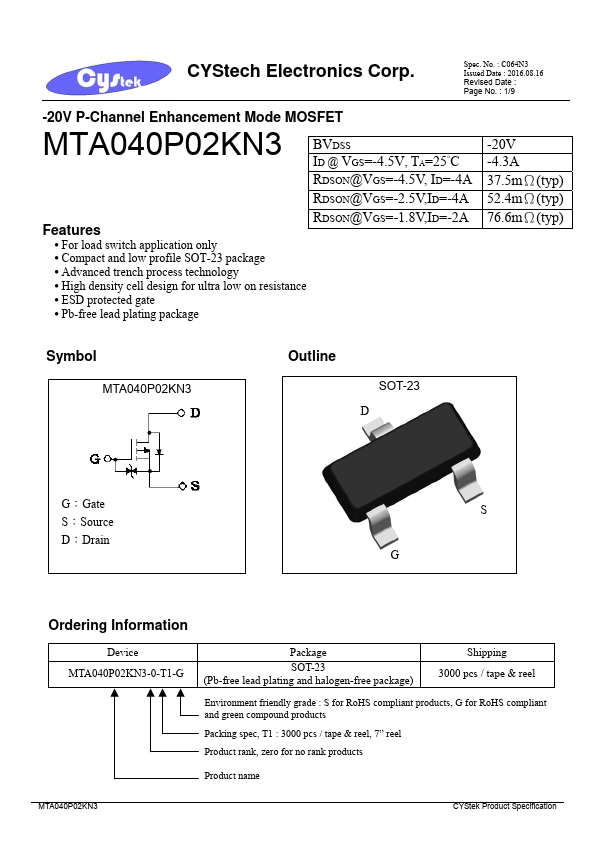
Symbol
MTA040P02KN3
Outline
SOT-23 D
G:Gate S:Source D:Drain
S G
Ordering Information
Device MTA040P02KN3-0-T1-G
Package
SOT-23 (Pb-free lead plating and halogen-free package)
Shipping 3000 pcs / tape & reel
Environment friendly grade : S for RoHS compliant products, G for RoHS compliant and green compound products
Packing spec, T1 : 3000 pcs / tape & reel, 7” reel
Product rank, zero for no rank products
Product name
MTA040P02KN3
CYStek Product Specification
CYStech Electronics Corp.
Spec. No. : C064N3 Issued Date : 2016.08.16
Revised Date : Page No. : 2/9
Absolute Maximum Ratings (Ta=25°C)
Parameter
Drain-Source
Voltage Gate-Source
Voltage
Continuous Drain Current @ TA=25°C , VGS=-4.5V (Note 4) Continuous Drain Current @ TA=70°C, VGS=-4.5V (Note 4) Pulsed Drain Current (Notes 1, 2) ESD susceptibility (Note 3)
Maximum Power Dissipation (Note 4) Linear Derating Factor
Operating Junction and Storage Temperature Range
Symbol VDS VGS
ID
IDM V...