CYStech Electronics Corp.
Spec. No. : C089N3 Issued Date : 2015.11.09
Revised Date : Page No. : 1/9
-14V P-Channel Enh...
CYStech Electronics Corp.
Spec. No. : C089N3 Issued Date : 2015.11.09
Revised Date : Page No. : 1/9
-14V P-Channel Enhancement Mode
MOSFET
MTA025P01SN3 BVDSS ID @ VGS=-4.5V, TA=25°C
RDSON@VGS=-4.5V, ID=-4A
RDSON@VGS=-2.5V,ID=-4A
RDSON@VGS=-1.8V,ID=-2A Features
Low gate charge Compact and low profile SOT-23 package Advanced trench process technology High density cell design for ultra low on resistance Pb-free lead plating package
-14V -5.6A
25.5mΩ(typ) 35.5mΩ(typ) 52.0mΩ(typ)
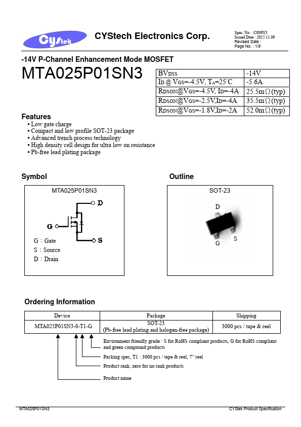
Symbol
MTA025P01SN3
Outline
SOT-23 D
G:Gate S:Source D:Drain
GS
Ordering Information
Device MTA025P01SN3-0-T1-G
Package
SOT-23 (Pb-free lead plating and halogen-free package)
Shipping 3000 pcs / tape & reel
Environment friendly grade : S for RoHS compliant products, G for RoHS compliant and green compound products
Packing spec, T1 : 3000 pcs / tape & reel, 7” reel
Product rank, zero for no rank products
Product name
MTA025P01SN3
CYStek Product Specification
CYStech Electronics Corp.
Spec. No. : C089N3 Issued Date : 2015.11.09
Revised Date : Page No. : 2/9
Absolute Maximum Ratings (Ta=25°C)
Parameter
Drain-Source
Voltage Gate-Source
Voltage Continuous Drain Current @ TA=25°C , VGS=-10V (Note 3) Continuous Drain Current @ TA=70°C, VGS=-10V (Note 3) Pulsed Drain Current (Notes 1, 2)
Maximum Power Dissipation (Note 3) Linear Derating Factor
Operating Junction and Storage Temperature Range
Symbol VDS VGS
ID IDM PD
Tj ; Tstg
Limits -14 ±12 -5.6 -4.5 -35
1.38
0.01 -55~+150
Unit V
...