(MT9LSDT872 / MT9LSDT1672) SYNCHRONOUS DRAM MODULE
www.DataSheet4U.com
ADVANCE
8, 16 MEG x 72 REGISTERED SDRAM DIMMs
SYNCHRONOUS DRAM MODULE
FEATURES
• JEDEC-standard 1...
Description
www.DataSheet4U.com
ADVANCE
8, 16 MEG x 72 REGISTERED SDRAM DIMMs
SYNCHRONOUS DRAM MODULE
FEATURES
JEDEC-standard 168-pin, dual in-line memory module (DIMM) PC133- and PC100-compliant Registered inputs with one-clock delay Phase-lock loop (PLL) clock driver to reduce loading Utilizes 133 MHz and 125 MHz SDRAM components ECC-optimized pinout 64MB (8 Meg x 72) and 128MB (16 Meg x 72) Single +3.3V ±0.3V power supply Fully synchronous; all signals registered on positive edge of PLL clock Internal pipelined operation; column address can be changed every clock cycle Internal SDRAM banks for hiding row access/ precharge Programmable burst lengths: 1, 2, 4, 8, or full page Auto Precharge and Auto Refresh Modes Self Refresh Mode 64ms, 4,096-cycle refresh LVTTL-compatible inputs and outputs Serial Presence-Detect (SPD)
MT9LSDT872, MT9LSDT1672
For the latest data sheet, please refer to the Micron Web site: www.micronsemi.com/datasheets/datasheet.html
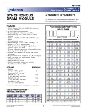
PIN ASSIGNMENT (FRONT VIEW) 168-PIN DIMM
OPTIONS
Package 168-pin DIMM (gold) Frequency/CAS Latency* 133 MHz/CL = 2 (7.5ns, 133 MHz SDRAMs) 133 MHz/CL = 3 (7.5ns, 133 MHz SDRAMs) 100 MHz/CL = 2 (8ns, 125 MHz SDRAM)
MARKING
G -13E -133 -10E
*Device latency only; extra clock cycle required due to input register.
KEY SDRAM COMPONENT TIMING PARAMETERS
MODULE MARKING -13E -133 -10E SPEED GRADE -7E -75 -8E CAS LATENCY 2 3 2 ACCESS TIME 5.4ns 5.4ns 6ns SETUP TIME 1.5ns 1.5ns 2ns HOLD TIME 0.8ns 0.8ns 1...
Similar Datasheet