16Mb: 1 MEG x16 EDO DRAM
EDO DRAM
MT4C1M16E5 – 1 Meg x 16, 5V MT4LC1M16E5 – 1 Meg x 16, 3.3V
For the latest data sheet...
16Mb: 1 MEG x16 EDO DRAM
EDO DRAM
MT4C1M16E5 – 1 Meg x 16, 5V MT4LC1M16E5 – 1 Meg x 16, 3.3V
For the latest data sheet, please refer to the Micron Web site: www.micron.com/products/datasheets/sdramds.html
FEATURES
JEDEC- and industry-standard x16 timing, functions, pinouts, and packages High-performance
CMOS silicon-gate process Single power supply (+3.3V ±0.3V or 5V ±10%) All inputs, outputs and clocks are TTL-compatible Refresh modes: RAS#-ONLY, CAS#-BEFORE-RAS# (CBR), HIDDEN; optional self refresh (S) BYTE WRITE access cycles 1,024-cycle refresh (10 row, 10 column addresses) Extended Data-Out (EDO) PAGE MODE access 5V-tolerant inputs and I/Os on 3.3V devices
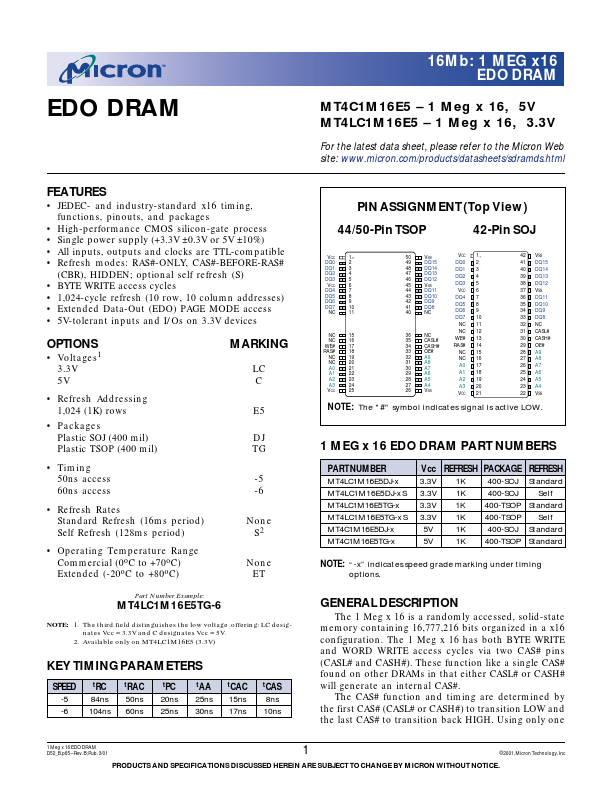
PIN ASSIGNMENT (Top View) 44/50-Pin TSOP
VCC DQ0 DQ1 DQ2 DQ3 VCC DQ4 DQ5 DQ6 DQ7 NC 1 2 3 4 5 6 7 8 9 10 11 50 49 48 47 46 45 44 43 42 41 40 VSS DQ15 DQ14 DQ13 DQ12 VSS DQ11 DQ10 DQ9 DQ8 NC
42-Pin SOJ
VCC DQ0 DQ1 DQ2 DQ3 VCC DQ4 DQ5 DQ6 DQ7 NC NC WE# RAS# NC NC A0 A1 A2 A3 VCC 1 2 3 4 5 6 7 8 9 10 11 12 13 14 15 16 17 18 19 20 21 42 41 40 39 38 37 36 35 34 33 32 31 30 29 28 27 26 25 24 23 22 VSS DQ15 DQ14 DQ13 DQ12 VSS DQ11 DQ10 DQ9 DQ8 NC CASL# CASH# OE# A9 A8 A7 A6 A5 A4 VSS
OPTIONS
Voltages 1 3.3V 5V Refresh Addressing 1,024 (1K) rows Packages Plastic SOJ (400 mil) Plastic TSOP (400 mil) Timing 50ns access 60ns access Refresh Rates Standard Refresh (16ms period) Self Refresh (128ms period) Operating Temperature Range Commercial (0oC to +70oC) Extended (-20oC to +80oC)
Part Number ...