www.DataSheet4U.com
2Mb SMART 3 BOOT BLOCK FLASH MEMORY
FLASH MEMORY
MT28F002B3 MT28F200B3
3V Only, Dual Supply (Smar...
www.DataSheet4U.com
2Mb SMART 3 BOOT BLOCK FLASH MEMORY
FLASH MEMORY
MT28F002B3 MT28F200B3
3V Only, Dual Supply (Smart 3)
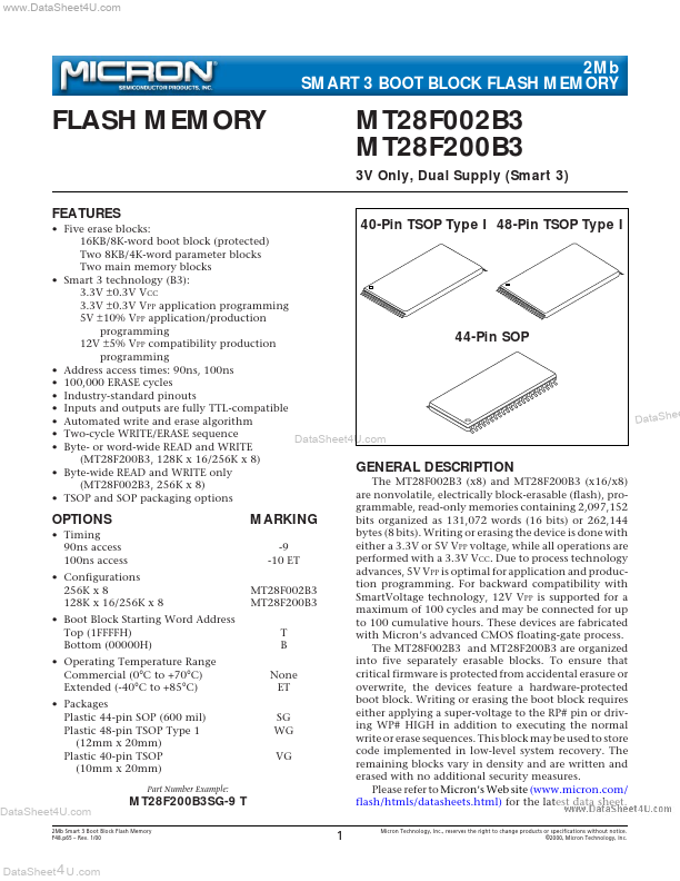
40-Pin TSOP Type I 48-Pin TSOP Type I Five erase blocks: 16KB/8K-word boot block (protected) Two 8KB/4K-word parameter blocks Two main memory blocks Smart 3 technology (B3): 3.3V ± 0.3V VCC 3.3V ± 0.3V VPP application programming 5V ±10% VPP application/production programming 44-Pin SOP 12V ± 5% VPP compatibility production programming Address access times: 90ns, 100ns 100,000 ERASE cycles Industry-standard pinouts Inputs and outputs are fully TTL-compatible ee DataSh Automated write and erase algorithm Two-cycle WRITE/ERASE sequence DataSheet4U.com Byte- or word-wide READ and WRITE (MT28F200B3, 128K x 16/256K x 8) GENERAL DESCRIPTION Byte-wide READ and WRITE only The MT28F002B3 (x8) and MT28F200B3 (x16/x8) (MT28F002B3, 256K x 8) are nonvolatile, electrically block-erasable (flash), pro TSOP and SOP packaging options grammable, read-only memories containing 2,097,152 bits organized as 131,072 words (16 bits) or 262,144 OPTIONS MARKING bytes (8 bits). Writing or erasing the device is done with Timing either a 3.3V or 5V VPP
voltage, while all operations are 90ns access -9 performed with a 3.3V VCC. Due to process technology 100ns access -10 ET advances, 5V VPP is optimal for application and produc Configurations tion programming. For backward compatibility with 256K x 8 MT28F002B3 Smart
Voltage technology, 12V VPP is supported for...