www.DataSheet4U.com
Freescale Semiconductor Technical Data
MRF9200L Rev. 1, 12/2004
RF Power Field Effect Transistors...
www.DataSheet4U.com
Freescale Semiconductor Technical Data
MRF9200L Rev. 1, 12/2004
RF Power Field Effect Transistors
N−Channel Enhancement−Mode Lateral
MOSFETs
Designed for broadband commercial and industrial applications with frequencies to 1000 MHz. The high gain and broadband performance of these devices make them ideal for large−signal, common−source amplifier applications in 26 volt base station equipment. Typical Single−Carrier N−CDMA Performance @ 880 MHz: VDD = 26 Volts, IDQ = 2400 mA, Pout = 40 Watts Avg., IS−95 CDMA (Pilot, Sync, Paging, Traffic Codes 8 Through 13). Channel Bandwidth = 1.2288 MHz. Peak/ Avg. Ratio = 9.8 dB @ 0.01% Probability on CCDF. Power Gain — 17.5 dB Drain Efficiency — 25% ACPR @ 750 kHz Offset — −46.5 dBc @ 30 kHz Bandwidth Capable of Handling 10:1 VSWR, @ 26 Vdc, 880 MHz, 40 Watts N−CDMA Output Power Characterized with Series Equivalent Large−Signal Impedance Parameters Internally Matched, Controlled Q, for Ease of Use Integrated ESD Protection Low Gold Plating Thickness on Leads, 40µ″ Nominal. In Tape and Reel. R3 Suffix = 250 Units per 56 mm, 13 inch Reel.
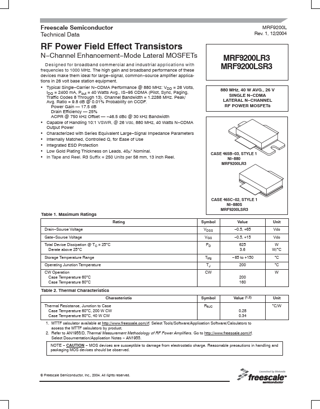
MRF9200LR3 MRF9200LSR3
880 MHz, 40 W AVG., 26 V SINGLE N−CDMA LATERAL N−CHANNEL RF POWER
MOSFETs
CASE 465B−03, STYLE 1 NI−880 MRF9200LR3
Table 1. Maximum Ratings
Rating Drain−Source
Voltage Gate−Source
Voltage Total Device Dissipation @ TC = 25°C Derate above 25°C Storage Temperature Range Operating Junction Temperature CW Operation Case Temperature 60°C Case Tempera...