MPSW45, MPSW45A
MPSW45A is a Preferred Device
One Watt Darlington Transistors
NPN Silicon
Features http://onsemi.com
CO...
MPSW45, MPSW45A
MPSW45A is a Preferred Device
One Watt Darlington Transistors
NPN Silicon
Features http://onsemi.com
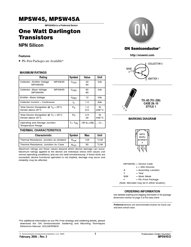
COLLECTOR 3 BASE 2 Symbol MPSW45 MPSW45 VCES VCBO VEBO IC PD PD TJ, Tstg Value 40 50 50 60 12 1.0 1.0 8.0 2.5 20 Unit Vdc Vdc Vdc Adc W mW/°C W mW/°C 1 2 3 TO−92 (TO−226) CASE 29−10 STYLE 1 EMITTER 1
Pb−Free Packages are Available*
MAXIMUM RATINGS
Rating Collector −Emitter
Voltage MPSW45A Collector −Base
Voltage MPSW45A Emitter −Base
Voltage Collector Current − Continuous Total Device Dissipation @ TA = 25°C Derate above 25°C Total Device Dissipation @ TC = 25°C Derate above 25°C Operating and Storage Junction Temperature Range
MARKING DIAGRAM
−55 towww.DataSheet4U.com +150 °C
THERMAL CHARACTERISTICS
Characteristic Thermal Resistance, Junction−to−Ambient Thermal Resistance, Junction−to−Case Symbol RqJA RqJC Max 125 50 Unit °C/W °C/W MPS W45x AYWW G G
Maximum ratings are those values beyond which device damage can occur. Maximum ratings applied to the device are individual stress limit values (not normal operating conditions) and are not valid simultaneously. If these limits are exceeded, device functional operation is not implied, damage may occur and reliability may be affected. MPSW45x = Device Code x = 45A Devices A = Assembly Location Y = Year WW = Work Week G = Pb−Free Package (Note: Microdot may be in either location)
ORDERING INFORMATION
See detailed ordering and shipping information in the package dimensions section on page 5 of this data sheet...