MPSA77
MPSA77
PNP Darlington Transistor
• This device is designed for applications requiring extremely high current gai...
MPSA77
MPSA77
PNP Darlington Transistor
This device is designed for applications requiring extremely high current gain at currents to 800mA. Sourced from process 61.
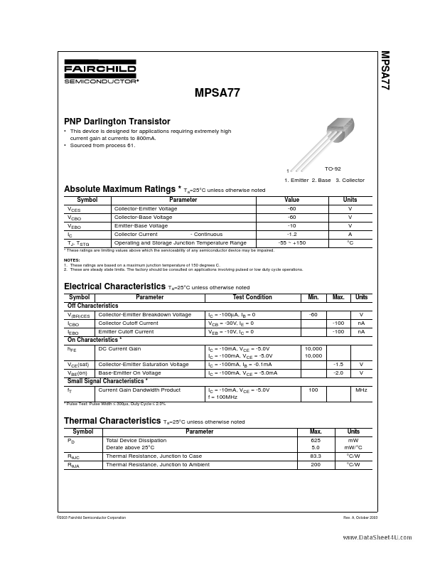
1
TO-92
1. Emitter 2. Base 3. Collector
Absolute Maximum Ratings * Ta=25°C unless otherwise noted
Symbol VCES VCBO VEBO IC TJ, TSTG Parameter Collector-Emitter
Voltage Collector-Base
Voltage Emitter-Base
Voltage Collector Current - Continuous Operating and Storage Junction Temperature Range Value -60 -60 -10 -1.2 -55 ~ +150 Units V V V A °C
* These ratings are limiting values above which the serviceability of any semiconductor device may be impaired. NOTES: 1. These ratings are based on a maximum junction temperature of 150 degrees C. 2. These are steady state limits. The factory should be consulted on applications involving pulsed or low duty cycle operations.
Electrical Characteristics Ta=25°C unless otherwise noted
Symbol Off Characteristics V(BR)CES ICBO IEBO hFE VCE(sat) VBE(on) fT Parameter Test Condition IC = -100µA, IB = 0 VCB = -30V, IE = 0 VEB = -10V, IC = 0 IC = -10mA, VCE = -5.0V IC = -100mA, VCE = -5.0V IC = -100mA, IB = -0.1mA IC = -100mA, VCE = -5.0mA IC = -10mA, VCE = -5.0V f = 100MHz 100 10,000 10,000 -1.5 -2.0 V V MHz Min. -60 -100 -100 Max. Units V nA nA Collector-Emitter Breakdown
Voltage Collector Cutoff Current Emitter Cutoff Current DC Current Gain Collector-Emitter Saturation
Voltage Base-Emitter On
Voltage Current Gain Dandwidth Product
On Characteristics *
Small Signal Chara...