MPF4392, MPF4393
JFET Switching Transistors
N−Channel − Depletion
Features
Pb−Free Packages are Available*
MAXIMUM RA...
MPF4392, MPF4393
JFET Switching Transistors
N−Channel − Depletion
Features
Pb−Free Packages are Available*
MAXIMUM RATINGS
Rating Drain −Source
Voltage Drain −Gate Voltag Gate−Source
Voltage Forward Gate Current Total Device Dissipation
@ TA = 25C Derate above 25C
Symbol VDS VDG VGS IG(f) PD
Value 30 30 30 50
350 2.8
Unit Vdc Vdc Vdc mAdc
mW mW/C
Operating and Storage Channel Temperature Range
Tchannel, − 65 to +150
C
Tstg
Stresses exceeding Maximum Ratings may damage the device. Maximum Ratings are stress ratings only. Functional operation above the Recommended Operating Conditions is not implied. Extended exposure to stresses above the Recommended Operating Conditions may affect device reliability.
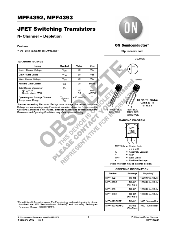
http://onsemi.com 2 SOURCE
3 GATE
1 DRAIN
123
STRAIGHT LEAD BULK PACK
1 2 3
TO−92 (TO−226AA) CASE 29−11 STYLE 5
BENT LEAD
TAPE & REEL AMMO PACK
MARKING DIAGRAM
MPF 439x AYWW G
G
*For additional information on our Pb−Free strategy and soldering details, please download the ON Semiconductor Soldering and Mounting Techniques Reference Manual, SOLDERRM/D.
Semiconductor Components Industries, LLC, 2012
1
February, 2012 − Rev. 6
MPF439x = Device Code
x = 2 or 3
A
= Assembly Location
Y
= Year
WW
= Work Week
G
= Pb−Free Package
(Note: Microdot may be in either location)
ORDERING INFORMATION
Device
Package
Shipping†
MPF4392
TO−92 1000 Units / Bulk
MPF4392G
TO−92 1000 Units / Bulk (Pb−Free)
MPF4393
TO−92 1000 Units / Bulk
MPF4393G
TO−92 ...