MN101C67
MN101C67D, MN101C67G
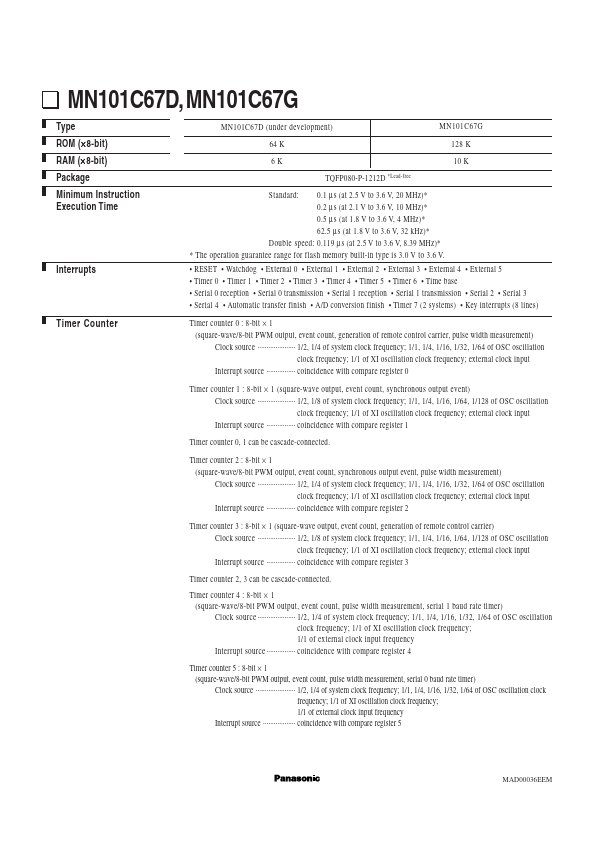
Type ROM (× 8-bit) RAM (× 8-bit) Package Minimum Instruction Execution Time
Standard: MN101C67D (un...
Description
MN101C67D, MN101C67G
Type ROM (× 8-bit) RAM (× 8-bit) Package Minimum Instruction Execution Time
Standard: MN101C67D (under development) 64 K 6K TQFP080-P-1212D
*Lead-free
MN101C67G 128 K 10 K
0.1 µ s (at 2.5 V to 3.6 V, 20 MHz)* 0.2 µ s (at 2.1 V to 3.6 V, 10 MHz)* 0.5 µ s (at 1.8 V to 3.6 V, 4 MHz)* 62.5 µ s (at 1.8 V to 3.6 V, 32 kHz)* Double speed: 0.119 µ s (at 2.5 V to 3.6 V, 8.39 MHz)* * The operation guarantee range for flash memory built-in type is 3.0 V to 3.6 V. RESET Watchdog External 0 External 1 External 2 External 3 External 4 External 5 Timer 0 Timer 1 Timer 2 Timer 3 Timer 4 Timer 5 Timer 6 Time base Serial 0 reception Serial 0 transmission Serial 1 reception Serial 1 transmission Serial 2 Serial 3 Serial 4 Automatic transfer finish A/D conversion finish Timer 7 (2 systems) Key interrupts (8 lines) Timer counter 0 : 8-bit × 1 (square-wave/8-bit PWM output, event count, generation of remote control carrier, pulse width measurement) Clock source ····················· 1/2, 1/4 of system clock frequency; 1/1, 1/4, 1/16, 1/32, 1/64 of OSC oscillation clock frequency; 1/1 of XI oscillation clock frequency; external clock input Interrupt source ················ coincidence with compare register 0 Timer counter 1 : 8-bit × 1 (square-wave output, event count, synchronous output event) Clock source ····················· 1/2, 1/8 of system clock frequency; 1/1, 1/4, 1/16, 1/64, 1/128 of OSC oscillation clock freque...
Similar Datasheet