MOTOROLA
SEMICONDUCTOR TECHNICAL DATA
Order this document by MMDF2N06VL/D
Product Preview
TMOS V™ SO-8 for Surface M...
MOTOROLA
SEMICONDUCTOR TECHNICAL DATA
Order this document by MMDF2N06VL/D
Product Preview
TMOS V™ SO-8 for Surface Mount
N–Channel Enhancement–Mode Silicon Gate
TMOS V is a new technology designed to achieve an on–resistance area product about one–half that of standard
MOSFETs. This new technology more than doubles the present cell density of our 50 and 60 volt TMOS devices. Just as with our TMOS E–FET designs, TMOS V is designed to withstand high energy in the avalanche and commutation modes. Designed for low
voltage, high speed switching applications in power supplies, converters and power motor controls, these devices are particularly well suited for bridge circuits where diode speed and commutating safe operating areas are critical and offer additional safety margin against unexpected
voltage transients. New Features of TMOS V On–resistance Area Product about One–half that of Standard
MOSFETs with New Low
Voltage, Low RDS(on) Technology Faster Switching than E–FET Predecessors
G S
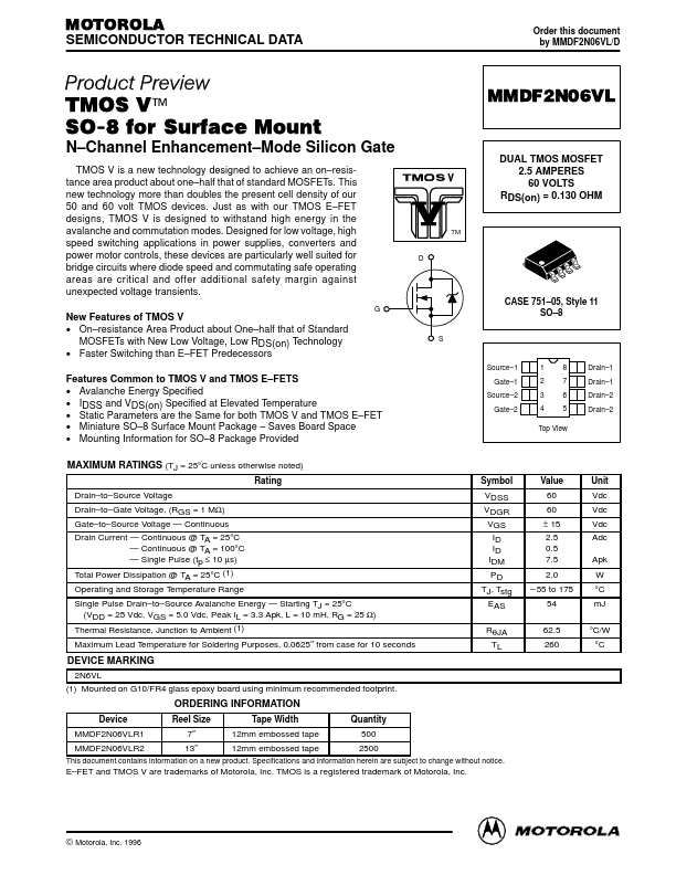
MMDF2N06VL
DUAL TMOS
MOSFET 2.5 AMPERES 60 VOLTS RDS(on) = 0.130 OHM
TM
D
CASE 751–05, Style 11 SO–8
Source–1
1 2 3 4
8 7 6 5
Drain–1 Drain–1 Drain–2 Drain–2
Features Common to TMOS V and TMOS E–FETS Avalanche Energy Specified IDSS and VDS(on) Specified at Elevated Temperature Static Parameters are the Same for both TMOS V and TMOS E–FET Miniature SO–8 Surface Mount Package – Saves Board Space Mounting Information for SO–8 Package Provided MAXIMUM RATINGS (TJ = 25°C u...