MOTOROLA
SEMICONDUCTOR TECHNICAL DATA
Order this document by MMBT2131T1/D
Product Preview
General Purpose Transistor...
MOTOROLA
SEMICONDUCTOR TECHNICAL DATA
Order this document by MMBT2131T1/D
Product Preview
General Purpose Transistors
PNP Bipolar Junction Transistor
(Complementary NPN Device: MMBT2132T1/T3)
NOTE:
Voltage and Current are negative for the PNP Transistor. MAXIMUM RATINGS (TC = 25°C unless otherwise noted)
Rating Collector–Emitter
Voltage Collector–Base
Voltage Emitter–Base
Voltage Collector Current Base Current Total Power Dissipation @ TC = 25°C Total Power Dissipation @ TC = 85°C Thermal Resistance — Junction to Ambient (1) Total Power Dissipation @ TC = 25°C Total Power Dissipation @ TC = 85°C Thermal Resistance — Junction to Ambient (2) Operating and Storage Temperature Range Symbol VCEO VCBO VEBO IC IB PD PD RqJA PD PD RqJA TJ, Tstg Value 30 40 5.0 700 350 342 178 366 665 346 188 – 55 to +150 Unit V V V mA mA mW mW °C/W mW mW °C/W °C
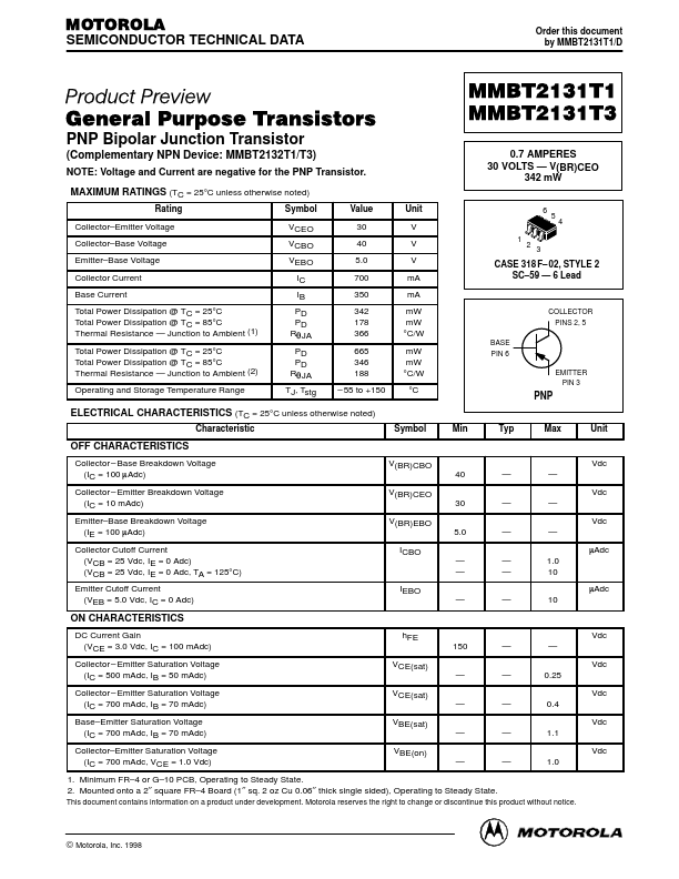
MMBT2131T1 MMBT2131T3
0.7 AMPERES 30 VOLTS — V(BR)CEO 342 mW
6
5
4
1
2
3
CASE 318 F– 02, STYLE 2 SC–59 — 6 Lead
COLLECTOR PINS 2, 5 BASE PIN 6 EMITTER PIN 3
PNP
Min Typ Max Unit
ELECTRICAL CHARACTERISTICS (TC = 25°C unless otherwise noted)
Characteristic Symbol
OFF CHARACTERISTICS
Collector – Base Breakdown
Voltage (IC = 100 mAdc) Collector – Emitter Breakdown
Voltage (IC = 10 mAdc) Emitter–Base Breakdown
Voltage (IE = 100 mAdc) Collector Cutoff Current (VCB = 25 Vdc, IE = 0 Adc) (VCB = 25 Vdc, IE = 0 Adc, TA = 125°C) Emitter Cutoff Current (VEB = 5.0 Vdc, IC = 0 Adc) V(BR)CBO 40 V(BR)CEO 30 V(BR)EBO 5.0 ICBO — — IEBO — — 10 — ...