MMBF4416A
MMBF4416A
N-Channel RF Amplifier
• This device is designed for RF amplifiers. • Sourced from process 50.
G
S...
MMBF4416A
MMBF4416A
N-Channel RF Amplifier
This device is designed for RF
amplifiers. Sourced from process 50.
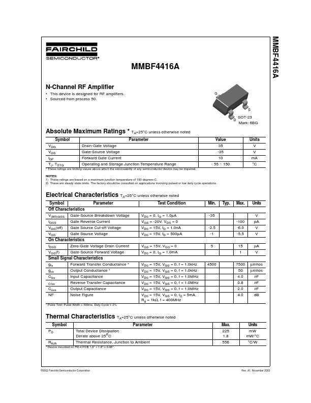
G
S D
SOT-23 Mark: 6BG
Absolute Maximum Ratings * TA=25°C unless otherwise noted
Symbol VDG VGS IGF TJ, TSTG Parameter Drain-Gate
Voltage Gate-Source
Voltage Forward Gate Current Operating and Storage Junction Temperature Range Value 35 -35 10 - 55 ~ 150 Units V V mA °C
* These ratings are limiting values above which the serviceability of any semiconductor device may be impaired. NOTES: 1) These ratings are based on a maximum junction temperature of 150 degrees C. 2) These are steady state limits. The factory should be consulted on applications involving pulsed or low duty cycle operations.
Electrical Characteristics TA=25°C unless otherwise noted
Symbol Parameter Test Condition VDS = 0, IG = 1.0µA VGS = -20V, VDS = 0 VDS = 15V, ID = 1.0nA VDS = 15V, ID = 500µA VGS = 15V, VGS = 0 VDS = 0, IG = 1.0mA VDS = 15V, VGS = 0, f = 1.0kHz VDS = 15V, VGS = 0, f = 1.0kHz VDS = 15V, VGS = 0, f = 1.0MHz VDS = 15V, VGS = 0, f = 1.0MHz VDS = 15V, VGS = 0, f = 1.0MHz VDS = 15V, VGS = 0, ID = 5mA, Rg = 1kΩ, f = 400MHz 4500 -2.5 -1 5 Min. -35 -100 -6.0 -5.5 15 1 7500 50 4.0 0.8 2.0 4.0 Typ. Max. Units V pA V V µA V µmhos µmhos
PF PF PF
Off Characteristics V(BR)GSS Gate-Source Breakdown
Voltage IGSS VGS(off) VGS Gate Reverse Current Gate Source Cut-off
Voltage Gate Source
Voltage
On Characteristics IDSS Zero-Gate
Voltage Drain Current VGS(f) Gate-Source Forward
Voltage Smal...