|
|
JFET Switching Transistors
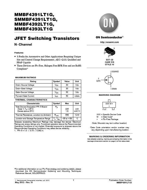
MMBF4391LT1G, SMMBF4391LT1G, MMBF4392LT1G, MMBF4393LT1G JFET Switching Transistors N−Channel Features • S Prefix for Au...
| @ 2014 :: Datasheetspdf.com :: Semiconductors datasheet search & download site. (Privacy Policy & Contact) |